An Ultra-Wideband Electromagnetic Absorbing Structure
An electromagnetic wave absorbing and ultra-broadband technology, applied in electrical components, antennas, etc., can solve the problems of limited application scope and little increase in bandwidth, and achieve the effect of ultra-broadband wave absorption.
- Summary
- Abstract
- Description
- Claims
- Application Information
AI Technical Summary
Problems solved by technology
Method used
Image
Examples
Embodiment Construction
[0019] The present invention will be further described below in conjunction with the accompanying drawings and embodiments, and the present invention includes but not limited to the following embodiments.
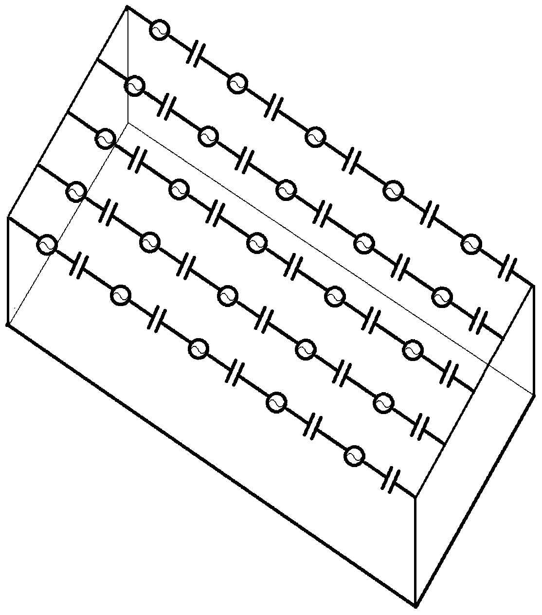
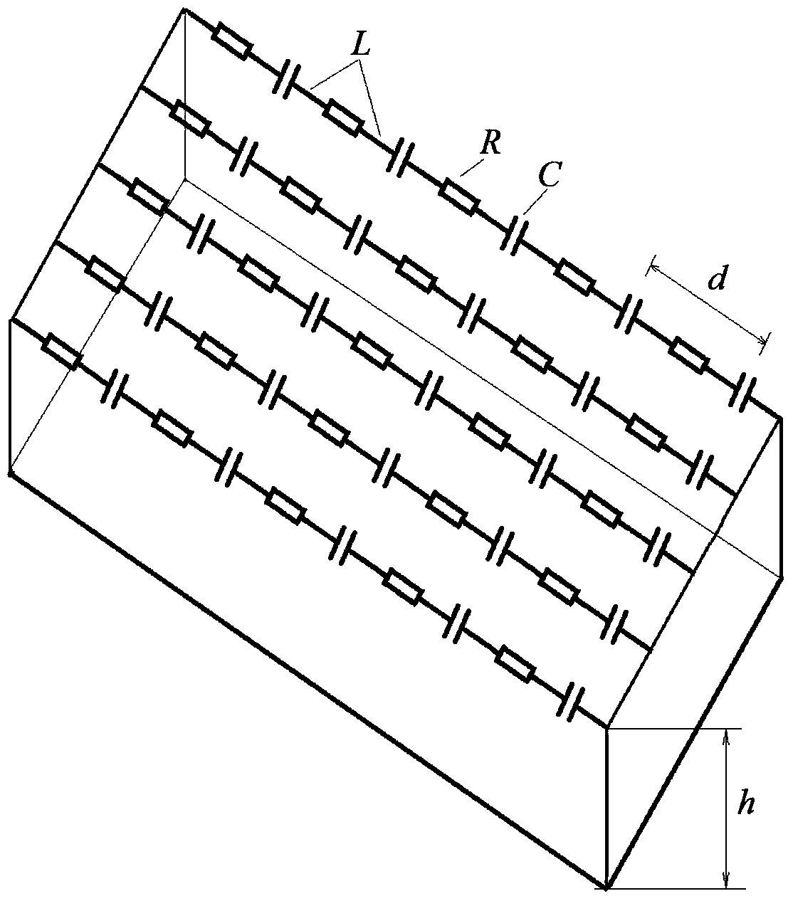
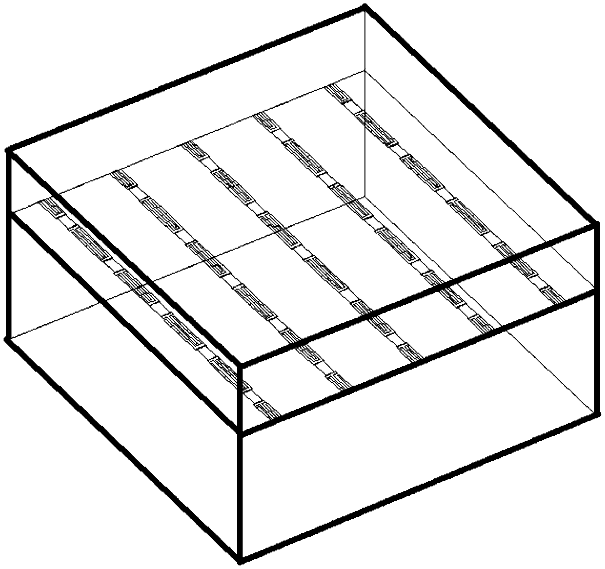
[0020] The electromagnetic absorbing structure is composed of a metal floor, an air layer, a tightly coupled array and a dielectric coating; the air layer is located between the metal floor and the tightly coupled array, and the tightly coupled array is arranged on the lower surface of the dielectric coating; the tightly coupled array is arranged periodically Composed of symmetrical vibrators; a resistor is welded to the center of each symmetrical vibrator (the matching resistance is given according to the input impedance of the center), and adjacent symmetrical vibrators are connected together through finger capacitance.
[0021] A tightly coupled array antenna can be implemented using a tightly coupled dipole antenna array, such as figure 1 shown. Will figure 1 The feed...
PUM
 Abstract
Description
Claims
Application Information


