
Miniature broadband metamaterial wave absorber

A technology of metamaterials and absorbers, applied in the field of electromagnetic metamaterials, can solve the problems of enhanced loss, high design cost, complex structure, etc.

Pending Publication Date: 2022-04-12
CHONGQING UNIV OF POSTS & TELECOMM
View PDF0 Cites 0 Cited by
  • Summary
  • Abstract
  • Description
  • Claims
  • Application Information

AI Technical Summary

Problems solved by technology

[0004] At present, some methods have been researched to realize broadband absorbers. The commonly used methods are: the unit combination method, which realizes a single-layer broadband absorber; the coherent and destructive method based on multilayer media, which realizes a multilayer absorber; Load concentrated components to enhance loss to realize broadband absorbing; broadband absorbers realized by these methods have problems such as complex structure, large volume, fine design, and high design cost

Method used


Image

  • Miniature broadband metamaterial wave absorber
  • Miniature broadband metamaterial wave absorber
  • Miniature broadband metamaterial wave absorber

Examples


Embodiment 1

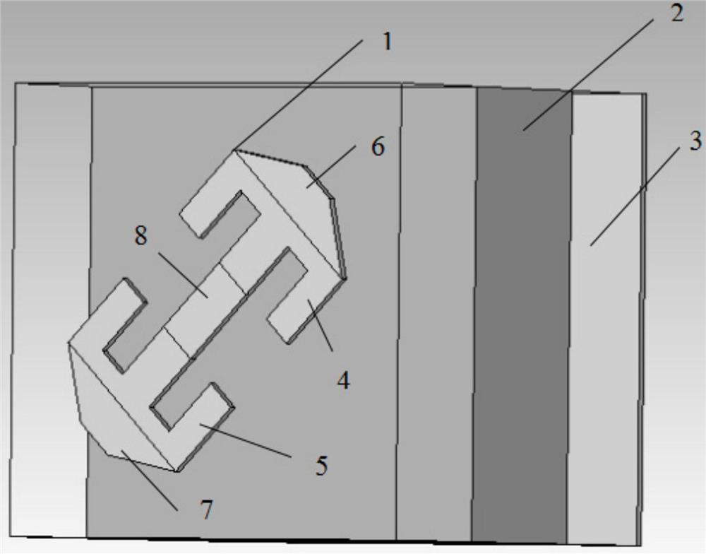
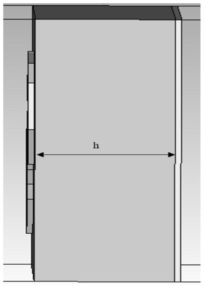
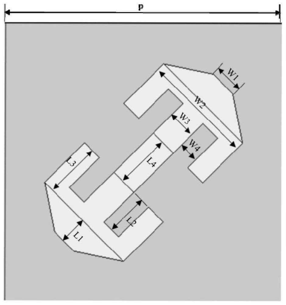
[0037] A miniature broadband metamaterial absorber, the microbroadband metamaterial absorber is a periodic structure, and each absorber periodic unit structure includes a three-layer structure including the first layer of metal structure layer 1 and the second layer of dielectric layer 2. The ground layer 3 of the third layer (such as figure 1 shown). The ground layer 3 has a thickness of 0.035mm; the thickness and side length of the dielectric layer 2 are respectively h=0.8mm (such as figure 2 As shown), p=2mm (such as image 3 shown); the metal structure layer 1 is composed of a "mountain"-shaped patch 4 with a thickness of 0.035mm, a trapezoidal patch 5 and a rectangular connecting patch 6;

[0038] The bottom of the "mountain"-shaped patch 4 is connected to the bottom of the trapezoidal patch 5, and then the "mountain"-shaped patch 4 is connected through a rectangular connection patch 6, and the rectangular connection patch 6 is located on the top of the "mountain"-shap...

Embodiment 2

[0043] A miniature broadband metamaterial absorber, the miniature broadband metamaterial absorber has a periodic structure, and a miniature broadband metamaterial absorber with 4x4 periodic unit structures is obtained, and other steps are the same as in Example 1.


PUM


Abstract

The invention discloses a miniature broadband metamaterial wave absorber, and belongs to the field of electromagnetic metamaterials. The miniature broadband metamaterial wave absorber is of a periodic structure, and each periodic unit structure comprises a first metal structure layer, a second dielectric layer and a third grounding layer. The metal structure layer is composed of two patches shaped like a Chinese character'shan ', two trapezoidal patches and a rectangular connecting patch. The bottoms of the two E-shaped patches are respectively connected with the lower bottom of the trapezoidal patch, then the two E-shaped patches are connected through the rectangular connecting patch, and the rectangular connecting patch is located in the middle of the top of the E-shaped patches; the metal structure layer is located in the middle of the dielectric layer and forms an angle of 45 degrees with the horizontal direction of the dielectric layer; the two E-shaped patches are connected by the rectangular patch to form a metal structure layer, and the structure meets central symmetry. The miniature broadband metamaterial wave absorber has the advantages of being small in size, wide in frequency band, simple in structure and excellent in wave absorbing performance.

Description

technical field [0001] The invention belongs to the field of electromagnetic metamaterials, in particular to a miniature broadband metamaterial absorber. Background technique [0002] Metamaterials refer to some composite materials with artificially designed structures and exhibit extraordinary physical properties that natural materials do not have. "Metamaterials" are a class of new materials that have emerged since the 21st century. These materials do not exist or are difficult to achieve in nature, and their special properties are also not available in natural materials. Due to its unique electromagnetic properties, electromagnetic metamaterials have been a research hotspot in the fields of physics and materials science. In recent years, with the continuous development of electromagnetic metamaterials, the theoretical research of metamaterials has become more and more mature, and its applications have become more and more extensive, covering various fields such as milita...

Claims


Application Information

Patent Timeline
Patent Type & Authority Applications(China)
IPC IPC(8): H01Q15/00H01Q17/00
Inventor 林峰周星宇王洋蒋建春张伟男谭沐莹
Owner CHONGQING UNIV OF POSTS & TELECOMM
Learn More