Array substrate, color-film substrate and touch display device

A technology for array substrates and color film substrates, applied in the field of color film substrates, touch display devices, and array substrates, can solve problems such as increased cost, increased thickness (increased volume, and low screen ratio of electronic equipment) to achieve screen ratio The effect of height and thickness

Active Publication Date: 2015-06-10
SHANGHAI TIANMA MICRO ELECTRONICS CO LTD +1
View PDF2 Cites 49 Cited by
  • Summary
  • Abstract
  • Description
  • Claims
  • Application Information

AI Technical Summary

Problems solved by technology

This simple superposition structure will cause problems such as low screen ratio, increased thickness (volume) and increased cost of electronic devices.

Method used


Image

  • Array substrate, color-film substrate and touch display device
  • Array substrate, color-film substrate and touch display device
  • Array substrate, color-film substrate and touch display device

Examples


Embodiment Construction

[0052] The following will clearly and completely describe the technical solutions in the embodiments of the present invention with reference to the accompanying drawings in the embodiments of the present invention. Obviously, the described embodiments are only some, not all, embodiments of the present invention. Based on the embodiments of the present invention, all other embodiments obtained by persons of ordinary skill in the art without making creative efforts belong to the protection scope of the present invention.

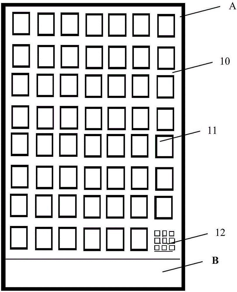
[0053] see figure 1 , the present invention provides an array substrate, comprising: a display area A and a non-display area B, the non-display area is provided with a plurality of gate lines, a plurality of data lines and drive chips, the display area is provided with a common The electrode layer 10, wherein, the gate line and the data line are insulated and intersect to define a plurality of pixel units arranged in an array, and the pixel unit includes: a pi...


PUM


Abstract

The invention provides an array substrate. The array substrate comprises a display region, a non-display region and a first fingerprint identifying unit, wherein the non-display region is provided with a plurality of gate lines, a plurality of data lines and a driving chip; the display region is provided with a common electrode layer; the gate lines and the data lines are intersected to one another in an insulated manner so as to define a plurality of pixel units which are distributed in an arrayed manner; each pixel unit comprises a pixel thin-film transistor and a pixel electrode; the common electrode layer comprises a plurality of first touch units which are insulated from one another; each first touch unit corresponds to a plurality of pixel units; and the first fingerprint identifying unit is used for identifying fingerprints. The array substrate comprises the fingerprint identifying unit. Compared with a simple fingerprint identifying device arranged in electronic equipment in the prior art, the array substrate with the fingerprint identifying device is high in screen occupation rate and is thin. The invention also provides a color-film substrate for identifying fingerprints and a touch display device of the color-film substrate.

Description

technical field [0001] The present invention relates to the display field, and more specifically, to an array substrate, a color filter substrate and a touch display device. Background technique [0002] With the continuous development of electronic equipment, fingerprint identification has become a major selling point of electronic equipment. Currently, common fingerprint identification devices are usually optical fingerprint sensing devices and semiconductor fingerprint sensing devices. Optical fingerprint sensing devices are usually bulky, and their applications are limited. The semiconductor fingerprint sensing device has the advantages of low price, small size and high recognition rate, and is more and more used in various electronic devices. [0003] The combination of the semiconductor fingerprint sensing device and the display device can undoubtedly bring a series of advanced functions, for example, the fingerprint recognition device can be used to safely perform o...

Claims


Application Information

Patent Timeline
Patent Type & Authority Applications(China)
IPC IPC(8): G06F3/041G06K9/00
CPCG06F3/0412G06F3/0443G06V40/1306
Inventor 孙云刚黄忠守杨康朴雪莹
Owner SHANGHAI TIANMA MICRO ELECTRONICS CO LTD
Why Eureka
Try Eureka