
Array substrate, display panel and display device

An array substrate and display panel technology, which is applied to instruments, computing, electrical and digital data processing, etc., can solve problems such as poor touch effect, improve touch effect and touch accuracy, ensure normal transmission of signals, reduce the effect of interference

Active Publication Date: 2015-07-22
SHANGHAI TIANMA MICRO ELECTRONICS CO LTD +1
View PDF6 Cites 25 Cited by
  • Summary
  • Abstract
  • Description
  • Claims
  • Application Information

AI Technical Summary

Problems solved by technology

However, the existing self-capacitive touch display device has poor touch effect

Method used


Image

  • Array substrate, display panel and display device
  • Array substrate, display panel and display device
  • Array substrate, display panel and display device

Examples


Embodiment Construction

[0048] The following will clearly and completely describe the technical solutions in the embodiments of the present invention with reference to the accompanying drawings in the embodiments of the present invention. Obviously, the described embodiments are only some of the embodiments of the present invention, not all of them. Based on the embodiments of the present invention, all other embodiments obtained by persons of ordinary skill in the art without making creative efforts belong to the protection scope of the present invention.

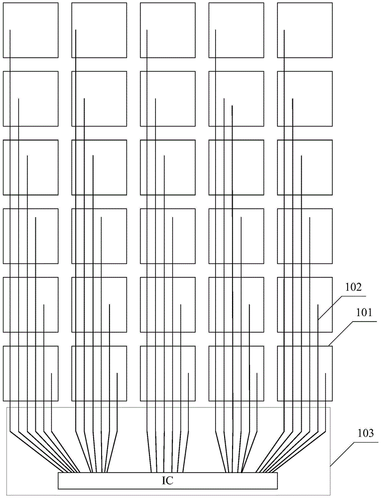
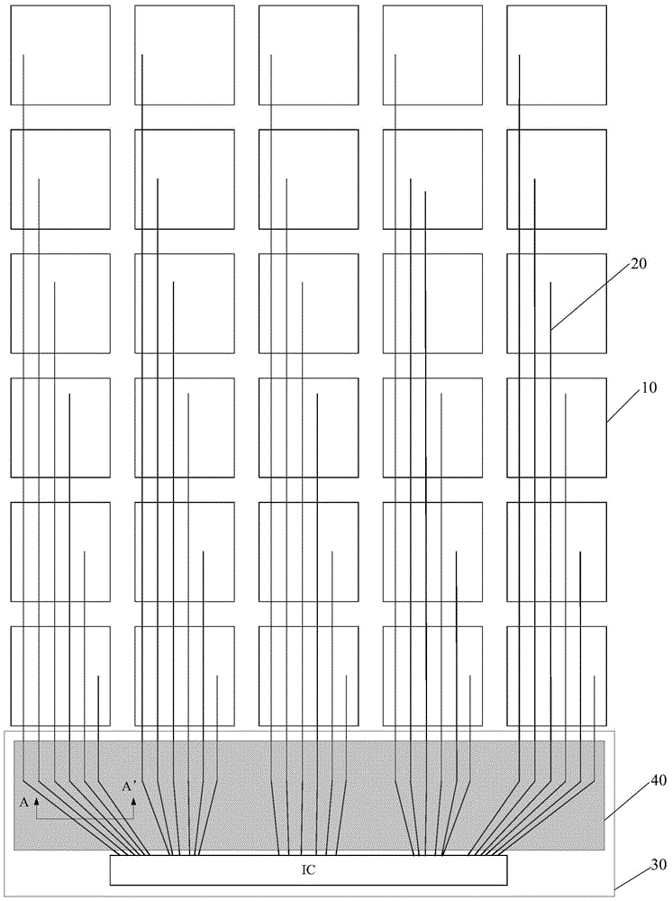
[0049] As mentioned in the background, the existing self-capacitive touch display devices have poor touch effects. The inventors found that when the touch operation is performed on the display device, the human hand or the external environment interferes with the part of the touch electrode lead wire located in the non-display area, which makes the signal transmitted by the touch electrode lead wire incorrect, resulting in poor touch effect .

...


PUM


Abstract

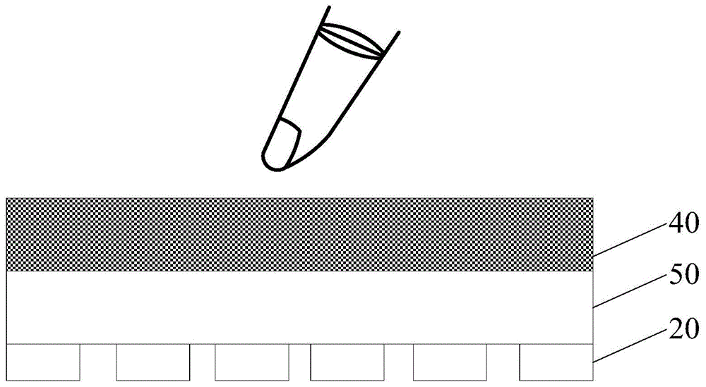
The invention discloses an array substrate, a display panel and a display device. The array substrate comprises a touch control layer, multiple touch control electrode lead wires and a shielding layer, wherein the touch control electrode lead wires are in electric connection with the touch control layer, and the touch control electrode lead wires extend to a non-display area of the array substrate; the shielding layer is arranged between a touch surface and the touch control electrode lead wires, wherein overlapping areas exist in the parts, located in the non-display area, of the shielding layer and the touch control electrode lead wires, and the shielding layer and the touch control electrode lead wires are insulated relative to one another. According to the technical scheme of the array substrate, the shielding layer is arranged between the touch surface and the touch control electrode lead wires so that interference of a hand or the external environment on the parts, located in the non-display area, of the touch control electrode lead wires can be weakened, it is guaranteed that the electrode lead wires transmit signals normally, and the touch control effect and the touch control precision of the display device are further improved; in addition, through the arrangement of the shielding layer, the touch control electrode lead wires covered with the shielding layer can be further protected from being damaged by static electricity, so that no damage is caused.

Description

technical field [0001] The present invention relates to the technical field of image display, and more specifically, to an array substrate, a display panel and a display device. Background technique [0002] In the initial stage of the development of the touch display, the touch display panel is formed by laminating the touch panel and the display panel to realize the touch display. The touch panel and the display panel need to be prepared separately, the cost is high, the thickness is relatively large, and the production efficiency is low. [0003] With the development of self-capacitive touch display integration technology, the common electrode layer of the array substrate in the display panel can also be used as the touch electrode layer for self-capacitive touch detection, and the touch can be performed in time-sequence through time-sharing driving Control and display control can realize touch and display functions at the same time. In this way, the touch electrodes ar...

Claims


Application Information

Patent Timeline
Patent Type & Authority Applications(China)
IPC IPC(8): G06F3/044G06F3/041
Inventor 孙云刚李谷骏
Owner SHANGHAI TIANMA MICRO ELECTRONICS CO LTD
Learn More