Array substrate and display panel

A technology of array substrates and data lines, applied in optics, instruments, electrical digital data processing, etc., can solve the problems of occupancy, inability to meet the needs of users for narrow borders, large non-display area 16 areas, etc., to reduce quantity and save The effect of non-display area area

Active Publication Date: 2015-08-05
XIAMEN TIANMA MICRO ELECTRONICS +1
View PDF8 Cites 38 Cited by
  • Summary
  • Abstract
  • Description
  • Claims
  • Application Information

AI Technical Summary

Problems solved by technology

[0004] figure 1 It is only illustrated by taking the extending direction of the sensing electrode 14 perpendicular to the extending direction of the data line 11 as an example. The sensing signal line 15 of the sensing electrode 14 is drawn from both sides, occupying a large area of ​​the non-display area 16
In addition, when the extending direction of the driving electrodes is perpendicular to the extending direction of the sensing electrodes and the extending direction of the driving electrodes is perpendicular to the extending direction of the data lines, the signal lines of the driving electrodes also need to be led out from one end of the driving electrodes, occupying 100% of the non-display area. area, so that the frame area of ​​the display panel is relatively large, which cannot meet the user's demand for narrow frame

Method used


Image

  • Array substrate and display panel
  • Array substrate and display panel
  • Array substrate and display panel

Examples


Embodiment Construction

[0021] In order to make the purpose, technical solutions and advantages of the present invention clearer, the technical solutions of the present invention will be clearly and completely described through implementation with reference to the accompanying drawings in the embodiments of the present invention. Obviously, the described embodiments are the embodiment of the present invention. Some, but not all, embodiments. Based on the embodiments of the present invention, all other embodiments obtained by persons of ordinary skill in the art without making creative efforts belong to the protection scope of the present invention.

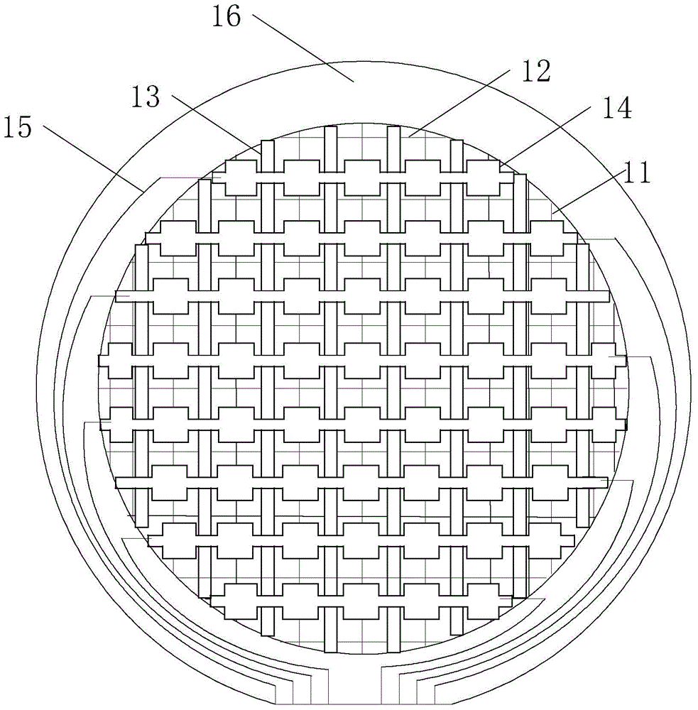
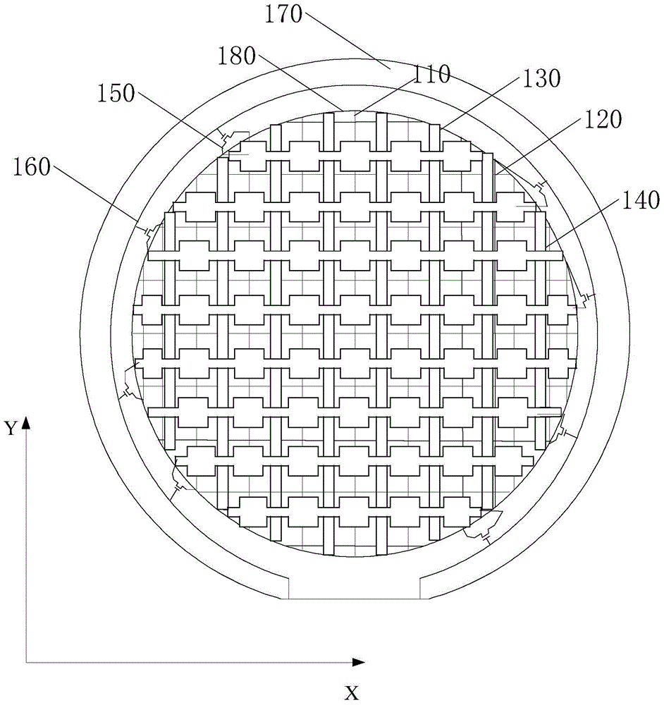
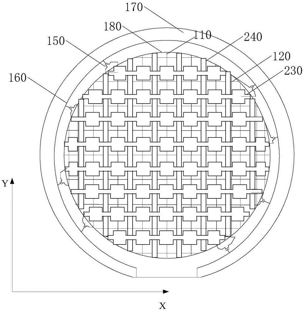
[0022] An embodiment of the present invention provides an array substrate, the array substrate includes: a plurality of data lines, a plurality of scan lines and touch electrodes. Wherein, a plurality of data lines and a plurality of scanning lines are insulated and intersect to define at least one sub-pixel unit, and the touch electrodes include driving...


PUM


Abstract

The invention discloses an array substrate and a display panel. The array substrate comprises a plurality of data lines, a plurality of scanning lines and touch electrodes. At least one subpixel unit is defined by the data lines and the scanning lines. The touch electrodes include driving electrodes and sensing electrodes, wherein the driving electrodes and the sensing electrodes are arranged in a mutual crossing mode. In the touch control stage, at least one touch electrode is communicated through the data lines so that driving signals or sensing signals can be transmitted to the communicated touch electrodes through the data lines. According to the array substrate, due to the fact that the data lines and at least one touch electrode are communicated in the touch control stage, the data lines further serve as signal lines for transmission of touch electrode signals, the number of the touch electrode signal lines in a non-display region of the display panel is reduced, the area, occupied by the touch electrode signal lines on the array substrate, of the non-display region is reduced, and the purpose of a narrow frame of the display panel is achieved.

Description

technical field [0001] The present invention relates to the field of display technology, in particular to an array substrate with a touch function and a display panel including the array substrate. Background technique [0002] In the field of display technology, more and more products integrate display and touch on the same display panel, which can effectively reduce the thickness of the display panel. The touch technology in the display panel usually includes capacitive, electromagnetic, etc. Among them, capacitive touch technology can be divided into self-capacitance and mutual capacitance. Mutual capacitive touch technology is to set the driving electrodes and sensing electrodes on the substrate, apply the driving signal on the driving electrodes during touch detection, and judge whether a touch occurs by detecting the sensing signal of the sensing electrodes, and determine the touch occurrence. Location. In the display panel, both the driving electrodes and the sensin...

Claims


Application Information

Patent Timeline
Patent Type & Authority Applications(China)
IPC IPC(8): G02F1/1343G02F1/1333G06F3/041
CPCG02F1/13338G02F1/134309G06F3/0412G06F3/04164G06F3/0445G06F3/0446
Inventor 颜华生
Owner XIAMEN TIANMA MICRO ELECTRONICS
Why Eureka
Try Eureka