
An organic electroluminescence touch panel, a driving method thereof, a display device

A touch panel and luminescent technology, which is applied in the direction of organic semiconductor devices, circuits, electrical components, etc., can solve the problems of affecting image display effect and uneven display brightness

Active Publication Date: 2017-10-10
BOE TECH GRP CO LTD +1
View PDF6 Cites 0 Cited by
  • Summary
  • Abstract
  • Description
  • Claims
  • Application Information

AI Technical Summary

Problems solved by technology

[0003] However, in the pixel circuit that drives the OLED to emit light, the threshold voltage V of the drive transistor in the pixel circuit will th There is inhomogeneity, which causes the current flowing through each pixel OLED to change, resulting in uneven display brightness, which affects the display effect of the entire image. In addition, generally, the embedded touch screen using self-capacitance touch technology Control panel, the touch electrode has parasitic capacitance, and its parasitic capacitance mainly comes from the signal lines used to transmit various control signals on the touch panel. Therefore, in order to improve the touch performance of the touch panel, it is necessary to reduce the parasitic capacitance of the touch electrode. capacitance

Method used


Image

  • An organic electroluminescence touch panel, a driving method thereof, a display device
  • An organic electroluminescence touch panel, a driving method thereof, a display device
  • An organic electroluminescence touch panel, a driving method thereof, a display device

Examples


Embodiment Construction

[0046] The specific implementation manners of the organic electroluminescence touch panel provided by the embodiments of the present invention, its driving method and the display device will be described in detail below with reference to the accompanying drawings.

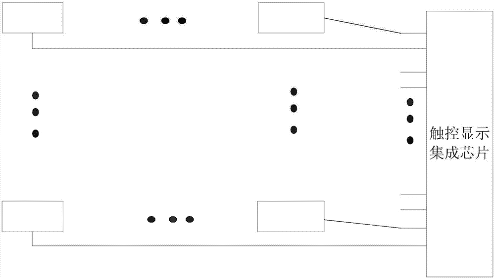
[0047] An embodiment of the present invention provides an organic electroluminescent touch panel, which may include: a pixel driving circuit and an organic electroluminescent structure; wherein,

[0048] like Figure 1a As shown, the organic electroluminescent structure may include: an anode layer 1, a cathode layer 2, and a light-emitting layer 3 located between the anode layer 1 and the cathode layer 2; wherein, the cathode layer 2 is divided into a plurality of mutually independent and insulated cathodes (The situation of the cathode layer partition is as follows Figure 1b As shown, the shape of the divided region of the cathode layer is not limited, and the shape of the cathode layer division can be determined...


PUM


Abstract

The invention discloses an organic electroluminescent touch panel, its driving method and a display device. On the basis of not changing the original organic electroluminescent structure, the cathode layer of the organic electroluminescent structure is divided to form multiple Independent and insulated cathode, in the touch stage, the cathode is used as a touch electrode to sense the external touch, and the touch signal is transmitted to the touch display integrated chip through the lead wire, so as to realize the integration of the display panel on the basis of organic electroluminescence display The touch function is realized, and the control terminal of the driving module is initialized in the reset stage through the pixel driving circuit, and the threshold voltage of the driving module is compensated in the compensation stage, which avoids the impact of the change of the threshold voltage of the driving module on the organic electroluminescent structure. At the same time, the signal on each signal line is synchronously modulated with the external touch signal induced by the touch electrode during the touch stage, which can eliminate the parasitic capacitance of the touch electrode and improve the touch performance of the touch panel.

Description

technical field [0001] The present invention relates to the field of display technology, in particular to an organic electroluminescence touch panel, a driving method thereof and a display device. Background technique [0002] With the advancement of display technology, more and more active matrix organic light emitting diode (Active Matrix Organic Light Emitting Diode, AMOLED) display panels have entered the market, compared with traditional transistor liquid crystal display panels (Thin Film Transistor Liquid Crystal Display, TFT LCD) In comparison, it has the advantages of low energy consumption, low production cost, self-illumination, wide viewing angle and fast response speed, and with the development of touch screen technology and market requirements, the overall module thinning is the market development trend, so the touch structure is composed of The touch sensor plug-in type develops to the touch sensor embedded type, so that the thickness of the touch panel can be ...

Claims


Application Information

Patent Timeline
Patent Type & Authority Patents(China)
IPC IPC(8): G09G3/3208
CPCG09G3/32G09G3/3233G09G2300/0819G09G2300/0861G09G2310/0251G09G2310/0262G09G2320/043G09G2354/00G06F3/0412G06F3/044G06F3/04184H10K59/40H10K59/80521H10K59/80523H10K50/11H10K50/15H10K50/16H10K50/81H10K50/822H10K59/131H10K2102/00H10K2102/103
Inventor 丁小梁董学王海生陈小川杨盛际刘英明刘伟王磊任涛
Owner BOE TECH GRP CO LTD
Learn More