
Array substrate, manufacturing method thereof, and display device

A technology of an array substrate and a manufacturing method, which is applied in the field of display and can solve problems such as the inability to realize borderless display

Active Publication Date: 2018-06-12
BOE TECH GRP CO LTD
View PDF4 Cites 0 Cited by
  • Summary
  • Abstract
  • Description
  • Claims
  • Application Information

AI Technical Summary

Problems solved by technology

For AMOLED display devices using GOA technology, GOA reduces the width of the Bonding area, but GOA still requires a certain area for wiring. Therefore, there are still some areas that cannot be displayed in the GOA circuit area. Due to the reduction of the size of GOA Faced with difficulties in technology and design, therefore, the existing AMOLED display devices can only reduce the border but cannot achieve borderless display

Method used


Image

  • Array substrate, manufacturing method thereof, and display device
  • Array substrate, manufacturing method thereof, and display device
  • Array substrate, manufacturing method thereof, and display device

Examples


Embodiment 1

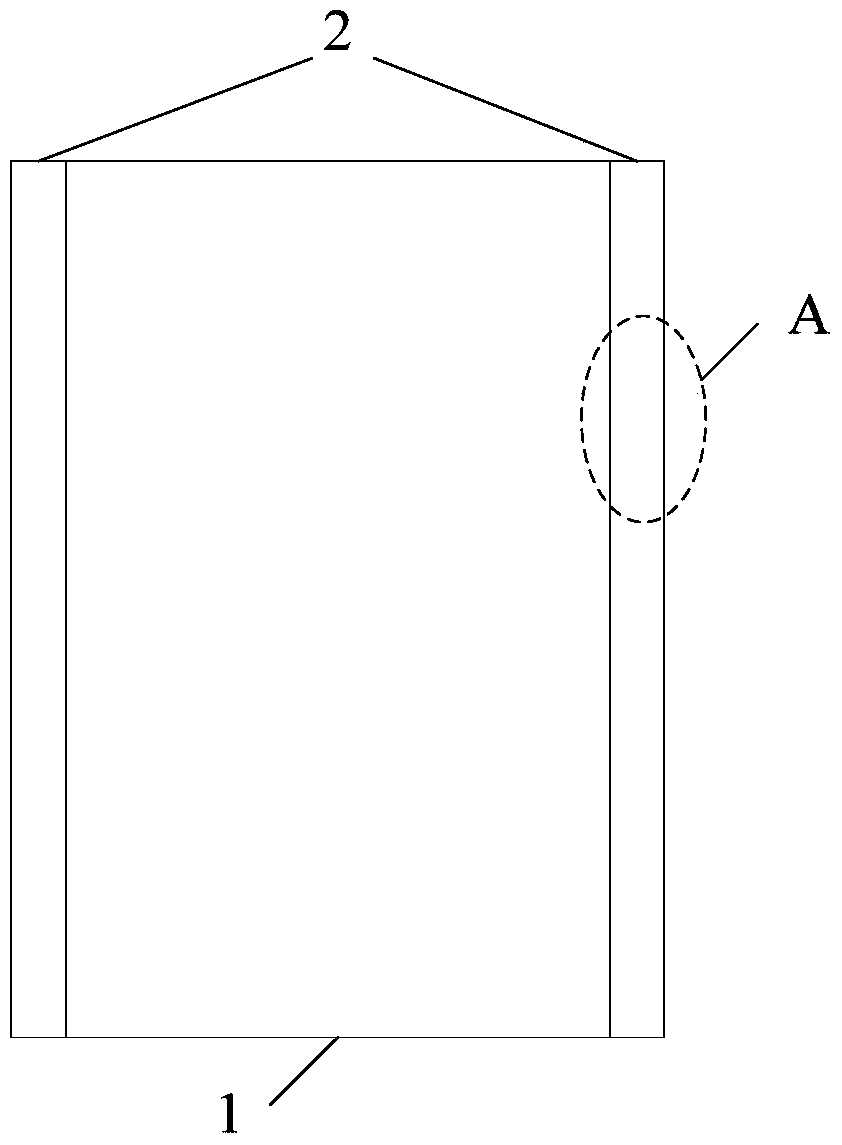
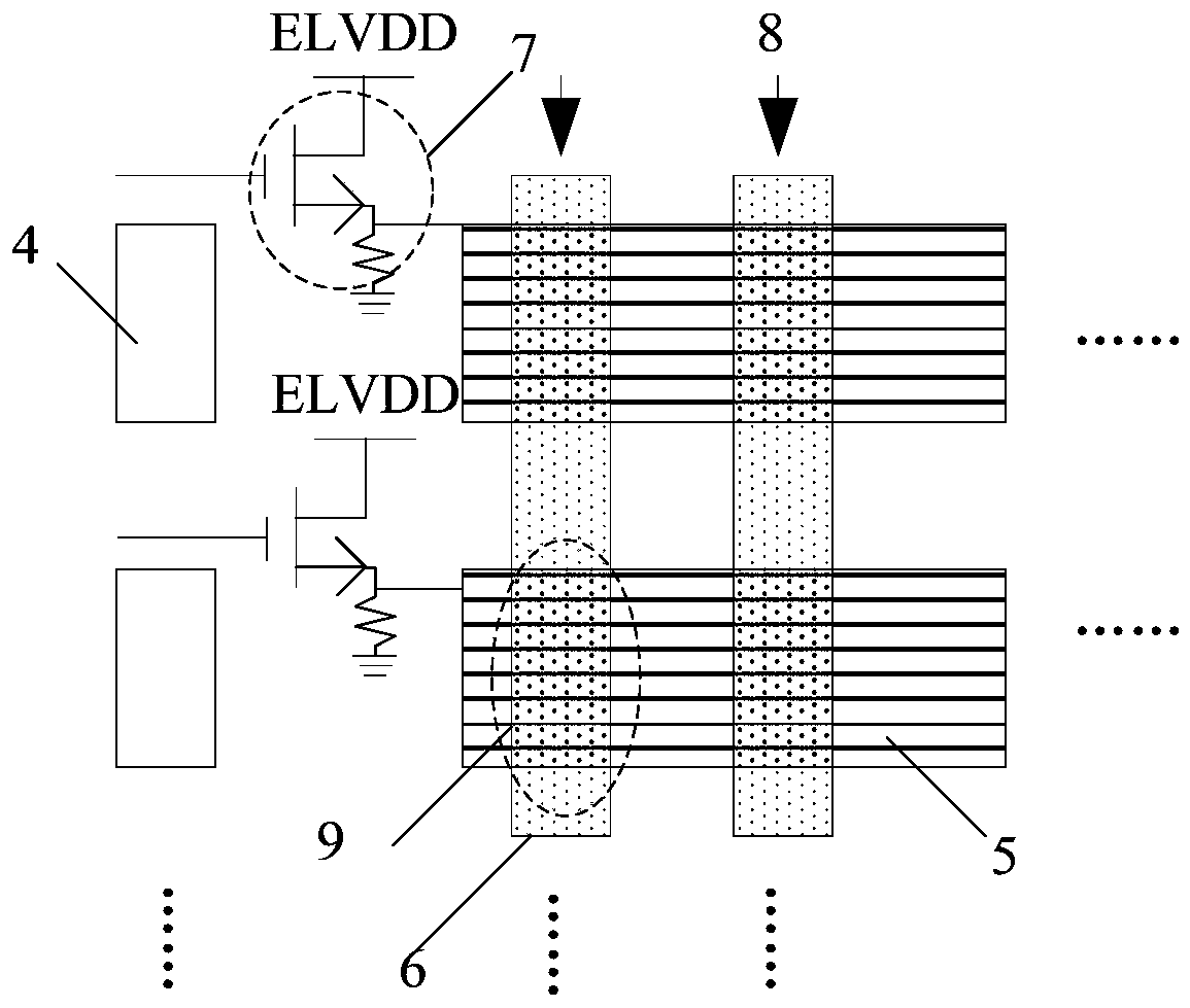
[0053] This embodiment provides an array substrate, including a display area and a gate electrode driving GOA circuit area outside the display area, wherein a passive matrix organic light emitting diode (PMOLED) display array is formed in the GOA circuit area.

[0054] For AMOLED display, each AMOLED display unit needs to be driven by a corresponding TFT (Thin Film Transistor), and there are many traces in the GOA circuit area of ​​the array substrate, and a TFT array cannot be formed in the GOA circuit area, so in the GOA area It is impossible to form an AMOLED display array; and for PMOLED display, each row of PMOLED display units is driven by a gate TFT. Taking advantage of this, this embodiment forms a PMOLED display array in the GOA circuit area, and the AMOLED display unit in the display area is connected. Connect and display images together, so that display can also be performed in the GOA circuit area, so as to realize narrow frame or no frame of the display device.

...

Embodiment 2

[0060] This embodiment provides a display device, including the above-mentioned array substrate. The display device may be any product or component with a display function such as a display panel, a television, a monitor, a digital photo frame, a mobile phone, a tablet computer, and the like.

Embodiment 3

[0062] This embodiment provides a method for manufacturing an array substrate. The array substrate includes a display area and a gate electrode driving GOA circuit area outside the display area. The manufacturing method includes:

[0063] A passive matrix organic light emitting diode PMOLED display array is formed in the GOA circuit area.

[0064] For AMOLED display, each AMOLED display unit needs to be driven by a corresponding TFT, and there are many traces in the GOA circuit area of ​​the array substrate, and the TFT array cannot be formed in the GOA circuit area, so AMOLED display cannot be formed in the GOA area. For PMOLED display, each row of PMOLED display units is driven by a gate TFT. Taking advantage of this, this embodiment forms a PMOLED display array in the GOA circuit area, and connects with the AMOLED display units in the display area to jointly display In this way, it can also be displayed in the GOA circuit area, so as to realize the narrow frame or no frame ...


PUM


Abstract

The invention provides an array substrate, a manufacturing method thereof, and a display device, belonging to the field of display technology. Wherein, the array substrate includes a display area and a gate electrode driving GOA circuit area outside the display area, and a passive matrix organic light emitting diode PMOLED display array is formed in the GOA circuit area. The technical solution of the present invention can realize narrow frame or even no frame of the display device.

Description

technical field [0001] The present invention relates to the field of display technology, in particular to an array substrate, a manufacturing method thereof, and a display device. Background technique [0002] Currently, flat panel display methods mainly include LCD (liquid crystal display), PDP (plasma display) and OLED (organic electroluminescence). Compared with LCD, OLED has the advantages of low power consumption, light weight, thin thickness, and foldability, so OLED may replace LCD as the new mainstream display technology. OLED drive can be divided into active drive (AMOLED) and passive drive (PMOLED). AMOLED can achieve large-size display, saves power and has high resolution, but the manufacturing process is complicated and requires high TFT stability; PMOLED has a relatively simple manufacturing process and simple structure, but it is difficult to achieve large-scale. [0003] In order to provide viewers with better visual enjoyment, narrow bezel displays are a po...

Claims


Application Information

Patent Timeline
Patent Type & Authority Patents(China)
IPC IPC(8): H01L27/32H01L21/77
CPCH10K59/123H10K59/128H10K59/176H10K59/17H10K50/813H10K50/822H10K50/828H10K59/00H10K59/122H10K59/124H10K59/131H10K59/179H10K59/1213H10K71/00H10K59/1201
Inventor 陈立强高涛高静许晨
Owner BOE TECH GRP CO LTD
Learn More