

Thin film packaging structure, display device and packaging method
A technology of thin film packaging and packaging substrates, which is applied in the fields of electric solid-state devices, semiconductor devices, semiconductor/solid-state device manufacturing, etc., and can solve problems such as not being too narrow, unfavorable narrow frames, and display panel frame width restrictions
- Summary
- Abstract
- Description
- Claims
- Application Information
AI Technical Summary
Problems solved by technology
Method used
Image

Examples
Embodiment Construction
[0036] In order to make the purpose, technical solutions and advantages of the embodiments of the present invention more clear, the following will clearly and completely describe the technical solutions of the embodiments of the present invention in conjunction with the drawings of the embodiments of the present invention. Apparently, the described embodiments are some, not all, embodiments of the present invention. All other embodiments obtained by those skilled in the art based on the described embodiments of the present invention belong to the protection scope of the present invention.
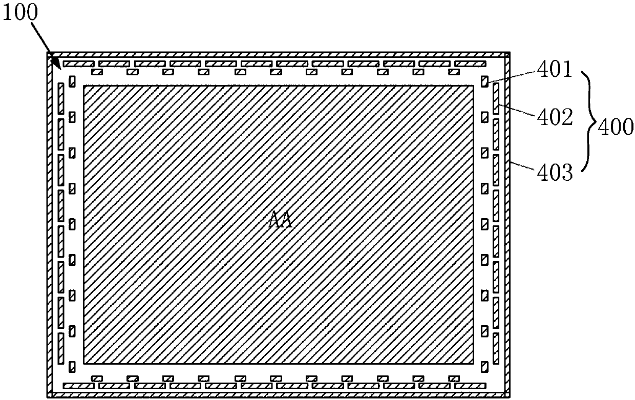
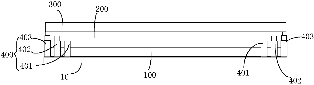
[0037] Aiming at the problem that the frame width cannot be too narrow due to the flow and diffusion of fluid organic materials in the OLED thin film packaging structure in the prior art, which is not conducive to the narrow frame, the embodiment of the present invention provides a thin film packaging structure, display device and The packaging method of the display device can not only ensu...
PUM
 Abstract
Description
Claims
Application Information