Patterning method and integrated circuit structure

Active Publication Date: 2010-10-14
MACRONIX INT CO LTD
View PDF3 Cites 167 Cited by
  • Summary
  • Abstract
  • Description
  • Claims
  • Application Information

AI Technical Summary

Benefits of technology

[0008]The present invention provides a patterning method, with which the purpo

Problems solved by technology

In the photolithography process, it is known that raising a line or space resolution beyond 65 nm, especially a line/space width of no more than 25/25 nm, in the current state of technology is rather d

Method used


Image

  • Patterning method and integrated circuit structure
  • Patterning method and integrated circuit structure
  • Patterning method and integrated circuit structure

Examples


Embodiment Construction

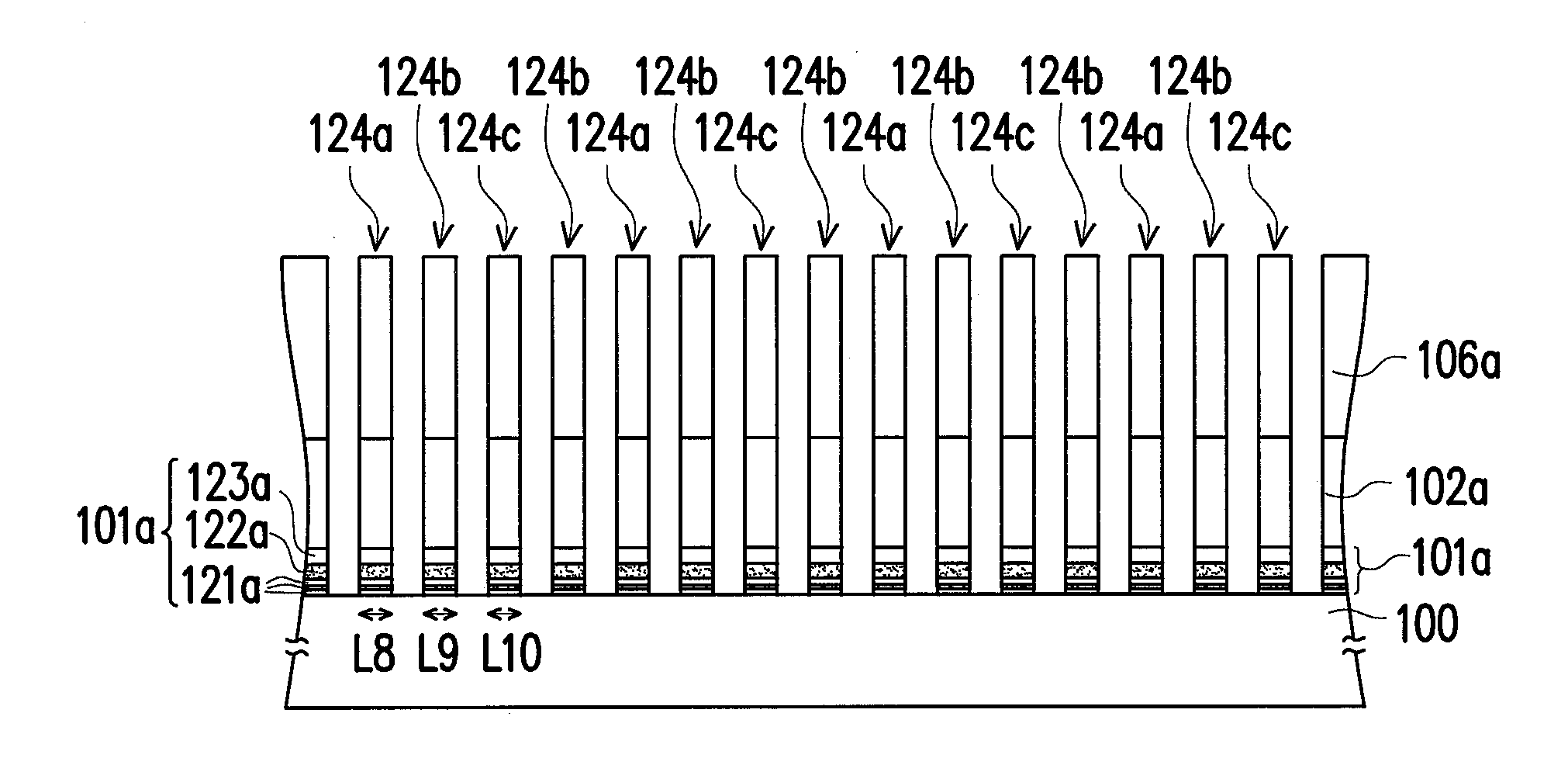
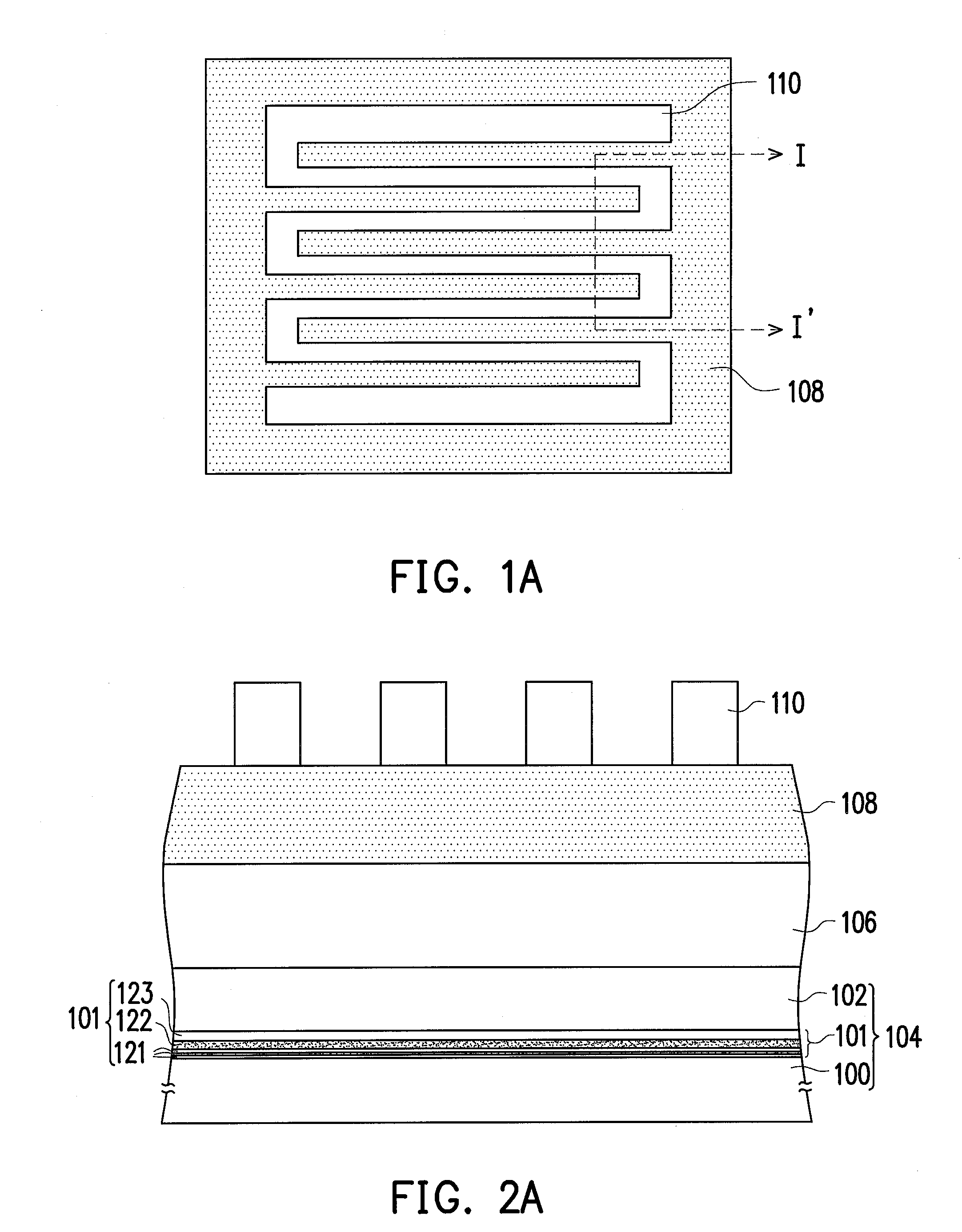
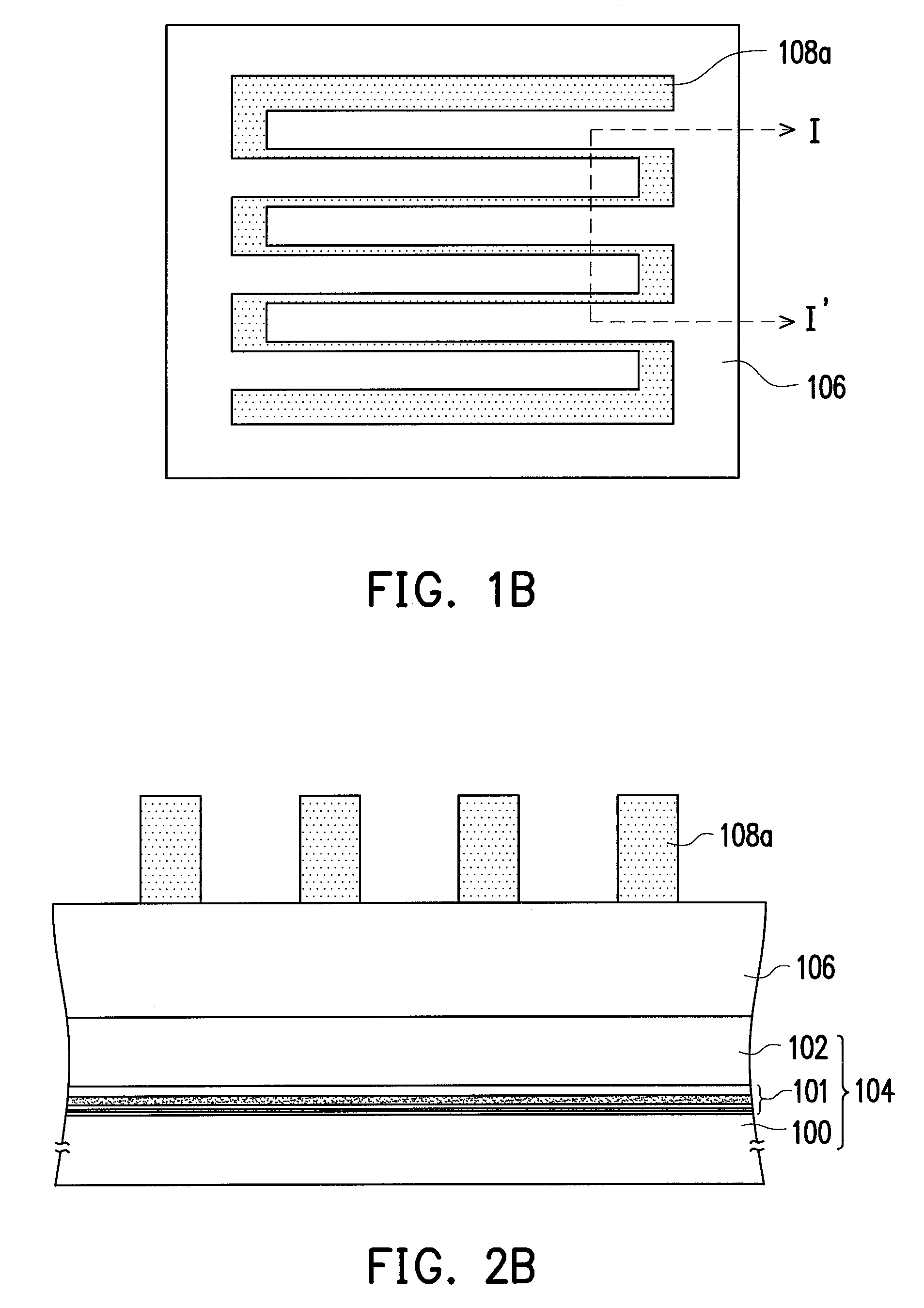
[0038]FIGS. 1A to 1I are schematic top views illustrating a patterning method according to an embodiment of the present invention FIGS. 2A to 2I are schematic cross-sectional views taken along the line I-I′ in FIGS. 1A to 1I.

[0039]Referring to FIGS. 1A and 2A, a mask layer 106, a transfer layer 108 and a patterned photoresist layer 110 are sequentially formed on a target layer 104. The target layer may be a stacked structure including a dielectric layer 101 and a material layer 102 sequentially formed on a substrate 100. The substrate 100 may be semiconductor substrate, such as a silicon substrate. The dielectric layer may be a single-layer or multi-layer structure. The material layer 102 includes polysilicon or metal, for example. The mask layer 106 includes TEOS-SiO2, BPSG, PSG, HSQ, FSG or USG, for example. The transfer layer 108 includes polysilicon or metal, for example. The dielectric layer 101, the material layer 102, the mask layer 106 and the transfer layer 108 are formed b...


PUM


Abstract

A patterning method is provided. First, a mask layer and a plurality of first transfer patterns are sequentially formed on a target layer. Thereafter, a plurality of second patterns is formed in the gaps between the first transfer patterns. Afterwards, a plurality of third transfer patterns is formed, wherein each of the third transfer patterns is in a gap between a first transfer pattern and a second transfer pattern adjacent to the first transfer pattern. A portion of the mask layer is then removed, using the first transfer patterns, the second transfer patterns and third transfer patterns as a mask, so as to form a patterned mask layer. Further, a portion of the target layer is removed using the patterned mask layer as a mask.

Description

BACKGROUND OF THE INVENTION[0001]1. Field of Invention[0002]The present invention relates to a patterning method and an integrated circuit structure.[0003]2. Description of Related Art[0004]Non-volatile memories provide the property of multiple entries, retrievals and erasures of data, and are able to retain the stored information even when the electrical power is off. As a result, non-volatile memories are widely used in personal computers and consumer electronic products.[0005]As the level of integration of a non-volatile memory is getting higher, the critical dimension of the same is getting smaller. Minimizing the critical dimension and increasing the level of integration have become the mainstream in the industry, and the key technology is in photolithography.[0006]In the photolithography process, it is known that raising a line or space resolution beyond 65 nm, especially a line / space width of no more than 25 / 25 nm, in the current state of technology is rather difficult, unles...

Claims


Application Information

Patent Timeline
IPC IPC(8): H01L29/00H01L21/302
CPCH01L21/0337H01L21/0338H01L21/32139H01L27/11568H01L27/11517H01L27/11521H01L27/115H10B41/00H10B69/00H10B41/30H10B43/30
Inventor LUE, HANG-TING
Owner MACRONIX INT CO LTD
Why Eureka
Try Eureka