Reduction of feature critical dimensions using multiple masks

a technology of feature critical dimensions and masks, applied in the field of semiconductor device formation, can solve the problems of limiting the density of conductive lines, and using shorter wavelength photoresists may provide additional problems, so as to and reduce the width of spaces

Inactive Publication Date: 2006-08-03
LAM RES CORP
View PDF29 Cites 196 Cited by
  • Summary
  • Abstract
  • Description
  • Claims
  • Application Information

AI Technical Summary

Benefits of technology

[0011] To achieve the foregoing and in accordance with the purpose of the present invention a method for forming features in an etch layer is provided. A first mask is formed over the etch layer wherein the first mask defines a plurality of spaces with widths. A sidewall layer is formed over the first mask wherein the sidewall layer reduces the widths of the spaces defined by the first mask. Features are etched into the etch layer through the sidewall layer, wherein the features have widths that are smaller than the widths of the spaces defined by the first mask. The mask and sidewall layer are removed. An additional feature step is performed, by performing the following steps. An additional mask is formed over the etch layer wherein the additional mask defines a plurality of spaces with widths. A sidewall layer is formed over the additional mask, wherein the sidewall layer reduces the widths of the spaces defined by the additional mask. Features are etched into the etch layer through the sidewall layer, wherein the widths of the feature are smaller than the widths of the spaces defined by the first mask. The mask and sidewall layer are removed.
[0012] In another manifestation of the invention, a method for forming features in an etch layer is provided. A first mask is formed over the etch layer wherein the first mask defines a plurality of spaces with widths and wherein the plurality of spaces have a critical dimension and a pitch. A sidewall layer is formed over the first mask wherein the sidewall layer reduces the widths of the spaces defined by the first mask. Features are etched into the etch layer through the sidewall layer, wherein the widths and critical dimension of the spaces is at least 50% less than the widths of the spaces and critical dimension of the spaces in the first mask. The mask and sidewall layer are removed. An additional feature step is performed by the following steps. An additional mask is formed over the etch layer wherein the additional mask defines a plurality of spaces with widths and wherein the plurality of spaces have a critical dimension and a pitch. A sidewall layer is formed over the additional mask, wherein the sidewall layer reduces the widths of the spaces defined by the additional mask. Features are etched into the etch layer through the sidewall layer, wherein the widths and critical dimension of the features are at least 50% less than the widths of the spaces and critical dimension of the spaces in the first mask and wherein the features have a pitch which is at least 50% less than the pitch of the spaces in the first mask and the pitch of the spaces in the additional mask. The mask and sidewall layer are removed. Additional masks can reduce the CD even more. For example 3 masks can provide about 65% and 4 masks can provide 75% shrink, and so on.

Problems solved by technology

Such tapering may provide unreliable features.
The use of shorter wavelength photoresists may provide additional problems over photoresists using longer wavelengths.
This may limit the density of the conductive lines that may be provided.

Method used


Image

  • Reduction of feature critical dimensions using multiple masks
  • Reduction of feature critical dimensions using multiple masks
  • Reduction of feature critical dimensions using multiple masks

Examples


Embodiment Construction

[0025] The present invention will now be described in detail with reference to a few preferred embodiments thereof as illustrated in the accompanying drawings. In the following description, numerous specific details are set forth in order to provide a thorough understanding of the present invention. It will be apparent, however, to one skilled in the art, that the present invention may be practiced without some or all of these specific details. In other instances, well known process steps and / or structures have not been described in detail in order to not unnecessarily obscure the present invention.

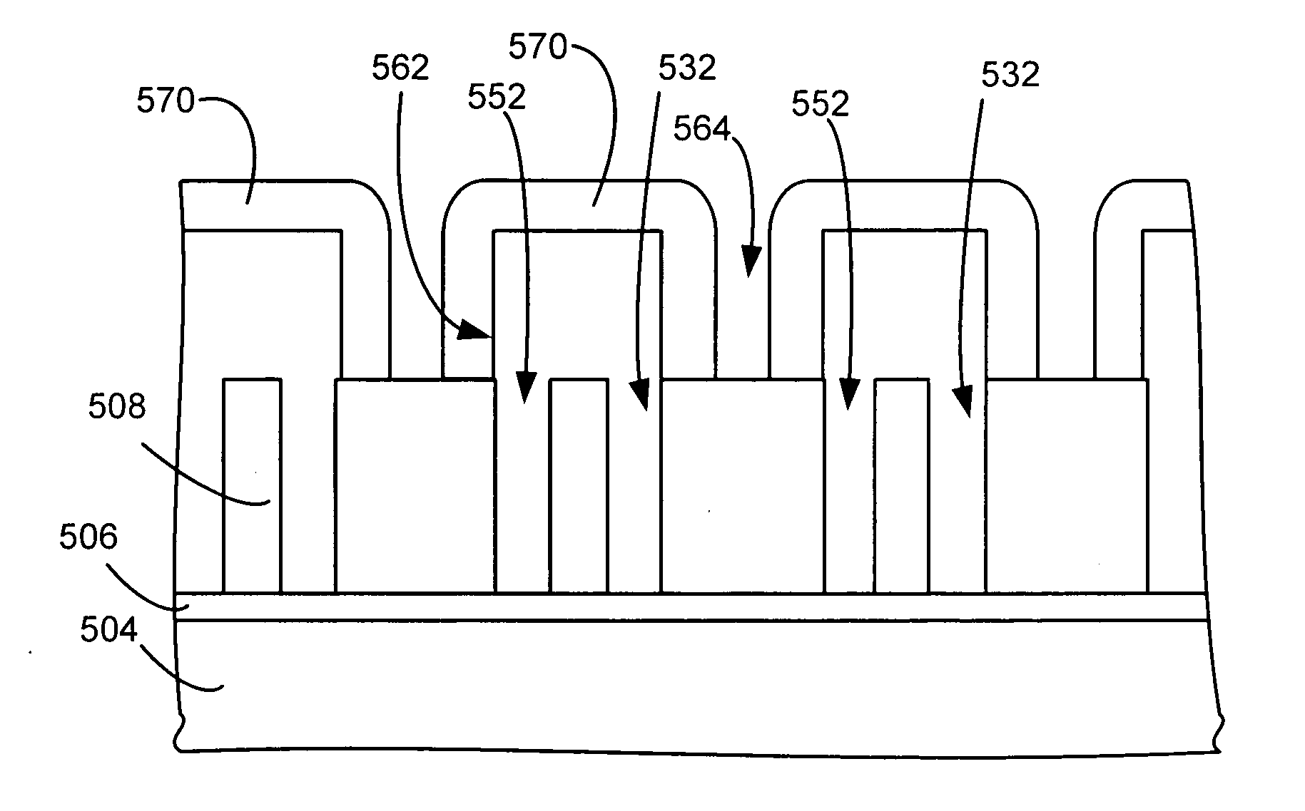
[0026] The invention provides features with small critical dimensions (CD). More specifically, the invention provides a features with CD's that are less than the CD of the photoresist pattern used to etch the feature.

[0027] To facilitate understanding, FIG. 3 is a high level flow chart of a process that may be used in an embodiment of the invention. A first feature step is performed (st...


PUM


Abstract

A method for forming features in an etch layer is provided. A first mask is formed over the etch layer wherein the first mask defines a plurality of spaces with widths. A sidewall layer is formed over the first mask. Features are etched into the etch layer through the sidewall layer, wherein the features have widths that are smaller than the widths of the spaces defined by the first mask. The mask and sidewall layer are removed. An additional mask is formed over the etch layer wherein the additional mask defines a plurality of spaces with widths. A sidewall layer is formed over the additional mask. Features are etched into the etch layer through the sidewall layer, wherein the widths that are smaller than the widths of the spaces defined by the first mask. The mask and sidewall layer are removed.

Description

BACKGROUND OF THE INVENTION [0001] The present invention relates to the formation of semiconductor devices. [0002] During semiconductor wafer processing, features of the semiconductor device are defined in the wafer using well-known patterning and etching processes. In these processes, a photoresist (PR) material is deposited on the wafer and then is exposed to light filtered by a reticle. The reticle is generally a glass plate that is patterned with exemplary feature geometries that block light from propagating through the reticle. [0003] After passing through the reticle, the light contacts the surface of the photoresist material. The light changes the chemical composition of the photoresist material such that a developer can remove a portion of the photoresist material. In the case of positive photoresist materials, the exposed regions are removed, and in the case of negative photoresist materials, the unexposed regions are removed. Thereafter, the wafer is etched to remove the u...

Claims


Application Information

Patent Timeline
Patent Type & Authority Applications(United States)
IPC IPC(8): H01L21/311
CPCH01L21/0273H01L21/3088H01L21/31144H01L21/32139H01L21/0337H01L21/0338
Inventor MARKS, JEFFREYSADJADI, S.M. REZA
Owner LAM RES CORP
Why Eureka
Try Eureka