
Electrodeformable thin film array, its preparation method and application
An electrostrictive and electrode array technology, which is applied in the manufacture/assembly of piezoelectric/electrostrictive devices, piezoelectric/electrostrictive/magnetostrictive devices, circuits, etc., can solve the problem of affecting unit deformation and electrical connection stability The performance cannot be well guaranteed, and the electrode leads occupy the film area, etc.
- Summary
- Abstract
- Description
- Claims
- Application Information
AI Technical Summary
Problems solved by technology
Method used
Image

Examples
preparation example Construction
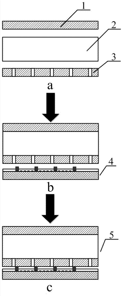
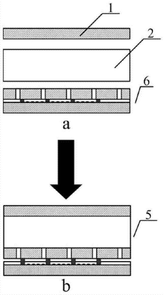
[0082] Another aspect of the present invention provides a method for preparing an electrodeformable thin film array, which mainly includes:
[0083] Provide core film, electrode film and electrode array;
[0084] Provides electrical connection layers including:
[0085] forming an electrical connection circuit with a predetermined structure on the substrate,
[0086] An electrical barrier layer is formed on the electrical connection circuit, and more than one through hole directly reaching the electrical connection circuit is formed on the electrical barrier layer,
[0087] Adding conductive material to the one or more through holes to form one or more electrical contact points, and electrically contacting the electrical contact points with selected points on the electrical connection line;
[0088] The electrode film, the core layer film, the electrode array and the electrical connection layer are sequentially arranged along the set direction, and the electrical contacts on...
Embodiment 1
[0138] Example 1 A method for preparing an electro-deformable film array based on a thermoplastic polyurethane core layer, comprising the following steps:
[0139] (1) Core layer film: The thermoplastic polyurethane and ionic liquid dispersion liquid is coated on the substrate, and the core layer film 2 with a thickness of 100 μm is peeled off from the substrate after evaporating the solvent.
[0140] (2) Electrode film: the metal Ag nanoparticle dispersion liquid was coated on the substrate, and the Ag nanopolymer electrode film 1 with a thickness of 5 μm was obtained after evaporating the solvent.
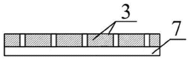
[0141] (3) Electrode array: as shown in FIG. 3 , after depositing the electrode film 1 on the substrate, the required electrode array pattern (electrode array 3 for short) is engraved on the substrate by laser engraving.
[0142] (4) Electrical connection layer: such as Figure 4a As shown, 4 μm polyethylene naphthalate (PEN) film 9 is used as the substrate, and the Figure 4b ...
Embodiment 2
[0147] Embodiment 2 A method for preparing an electro-deformable film array based on an ionomer Nafion core layer, comprising the following steps:
[0148] (1) Core layer membrane: Nafion ionic membrane and ionic liquid dispersion are coated on the substrate, and the solvent is evaporated and peeled off from the substrate to obtain a 100 μm thick core layer membrane 2 .
[0149] (2) Electrode film: Dissolve graphene and carbon nanotubes in an organic solvent in a certain proportion to form a dispersion liquid, coat the dispersion liquid on the substrate 7, and form a graphene / carbon nanotube film with a certain thickness after evaporating the solvent. Put the graphene / carbon nanotube film into an alkaline solution of ammonium salt and nickel salt, keep warm, wash, and anneal to obtain a nickel oxide-graphene / carbon nanotube nanoelectrode film 1 with a thickness of 5 μm.
[0150] (3) Electrical connection layer: see Figure 4a As shown, 4 μm polyethylene naphthalate (PEN) film...
PUM
 Abstract
Description
Claims
Application Information