Electro-deformation thin film array and preparation method and application thereof

A technology of electrostriction and electrode array, which is applied in the manufacture/assembly of piezoelectric/electrostrictive devices, piezoelectric/electrostrictive/magnetostrictive devices, circuits, etc. Connection stability cannot be well guaranteed, unfavorable array design and other issues

Active Publication Date: 2015-09-16
SUZHOU INST OF NANO TECH & NANO BIONICS CHINESE ACEDEMY OF SCI
View PDF12 Cites 16 Cited by
  • Summary
  • Abstract
  • Description
  • Claims
  • Application Information

AI Technical Summary

Problems solved by technology

[0006] However, there are very few technological methods related to lead wires. In the existing research, one method is to directly connect wires to each deformation unit. Because the wires have a certain quality and binding force, not only the deformation of the unit is greatly affected, but also the stability of the electrical connection. It cannot be well guaranteed; another method is to design a special-shaped unit structure, and extend the electrodes of the deformation unit to the edge of the film to apply voltage. In this method, the electrode leads will occupy a certain film area, which is not conducive to large-scale array design

Method used


Image

  • Electro-deformation thin film array and preparation method and application thereof
  • Electro-deformation thin film array and preparation method and application thereof
  • Electro-deformation thin film array and preparation method and application thereof

Examples


preparation example Construction

[0082] Another aspect of the present invention provides a method for preparing an electrodeformable thin film array, which mainly includes:

[0083] Provide core film, electrode film and electrode array;

[0084] Provides electrical connection layers including:

[0085] forming an electrical connection circuit with a predetermined structure on the substrate,

[0086] An electrical barrier layer is formed on the electrical connection circuit, and more than one through hole directly reaching the electrical connection circuit is formed on the electrical barrier layer,

[0087] Adding conductive material to the one or more through holes to form one or more electrical contact points, and electrically contacting the electrical contact points with selected points on the electrical connection line;

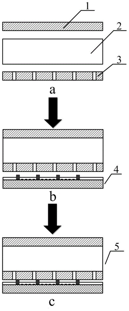
[0088] The electrode film, the core layer film, the electrode array and the electrical connection layer are sequentially arranged along the set direction, and the electrical contacts on...

Embodiment 1

[0138] Example 1 A method for preparing an electro-deformable film array based on a thermoplastic polyurethane core layer, comprising the steps of:

[0139] (1) Core layer film: The thermoplastic polyurethane and ionic liquid dispersion liquid is coated on the substrate, and the core layer film 2 with a thickness of 100 μm is peeled off from the substrate after evaporating the solvent.

[0140] (2) Electrode film: the metal Ag nanoparticle dispersion liquid was coated on the substrate, and the Ag nanopolymer electrode film 1 with a thickness of 5 μm was obtained after evaporating the solvent.

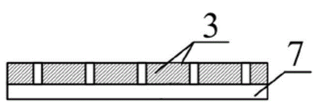
[0141] (3) Electrode array: as shown in FIG. 3 , after depositing the electrode film 1 on the substrate, the required electrode array pattern (electrode array 3 for short) is engraved on the substrate by laser engraving.

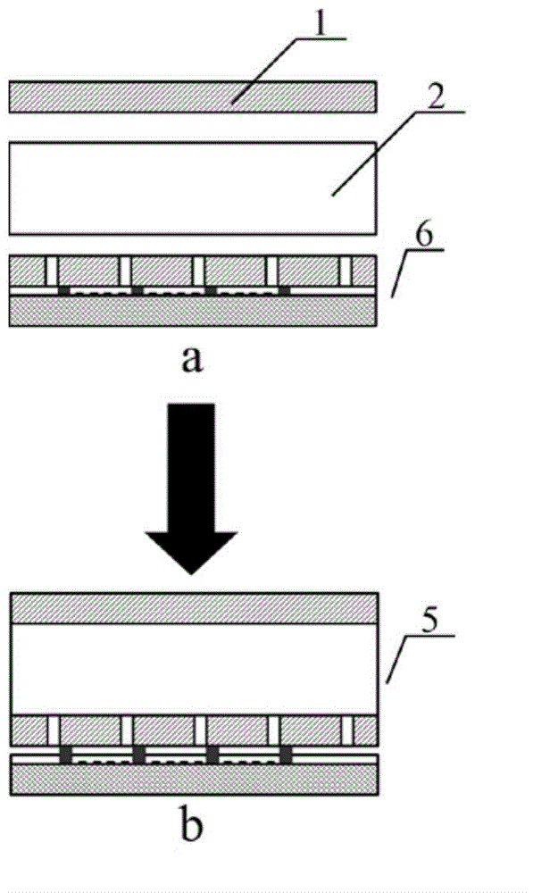
[0142] (4) Electrical connection layer: such as Figure 4a As shown, 4 μm polyethylene naphthalate (PEN) film 9 is used as the substrate, and the Figure 4b The ...

Embodiment 2

[0147] Example 2 A method for preparing an electro-deformable film array based on an ionic polymer Nafion core layer, comprising the steps of:

[0148] (1) Core layer membrane: Nafion ionic membrane and ionic liquid dispersion are coated on the substrate, and the solvent is evaporated and peeled off from the substrate to obtain a 100 μm thick core layer membrane 2 .

[0149] (2) Electrode film: Dissolve graphene and carbon nanotubes in an organic solvent in a certain proportion to form a dispersion liquid, coat the dispersion liquid on the substrate 7, and form a graphene / carbon nanotube film with a certain thickness after evaporating the solvent. Put the graphene / carbon nanotube film into an alkaline solution of ammonium salt and nickel salt, keep warm, wash, and anneal to obtain a nickel oxide-graphene / carbon nanotube nanoelectrode film 1 with a thickness of 5 μm.

[0150] (3) Electrical connection layer: see Figure 4a As shown, 4 μm polyethylene naphthalate (PEN) film ...


PUM


Abstract

The invention discloses an electro-deformation thin film array and a preparation method and application thereof. The thin film array comprises an electrode film, a core-layer film, an electrode array and an electric connection layer. The electric connection layer comprises an electric connection line, an electrical barrier layer and a plurality of electric contacts, wherein one end of each electric contact passes through the electrical barrier layer and is electrically contacted with each selected site of the electric connection line; the electrode film, the core-layer film, the electrode array and the electric connection layer are stacked in sequence; and the other end of each electric contact is electrically contacted with each set site on the electrode array. The preparation method of the thin film array comprises carrying out processing to form structure layers above respectively, and then, carrying out heating and pressurization combination to obtain the target product. Through the design above, components do not influence each other during processing, and unit quantity scale of the electro-deformation thin film array can be improved greatly. The electro-deformation thin film array can be applied to the fields of braille display, graphics safegurard and key, distorting mirror, three-dimensional graphic display, man-machine interface and pressure imaging and the like, and has a wide application value.

Description

technical field [0001] The invention specifically relates to an electro-deformable film array, its preparation method and application, and belongs to the field of material science. Background technique [0002] Electrodeformable film material is an ion-type electrically actuated deformation material, which has outstanding advantages such as light weight, good flexibility, low driving voltage, rapid response and large deformation. It can be used to make deformation devices and mechanical sensing devices. It is a new type of intelligent material that has emerged in the past two decades and has great application potential. [0003] Electrodeformable film materials are usually used as a whole in strips or blocks. For example, Japan’s EAMEX company has developed a robotic fish product that uses the bending deformation of strip materials to push fish to swim; The repeated vibration deformation of thin film strip materials simulates the flying action of birds; American M. Shahinpo...

Claims


Application Information

Patent Timeline
Patent Type & Authority Applications(China)
IPC IPC(8): H01L41/047H01L41/29
Inventor 陈韦朱子才胡颖武观蓝天刘洋
Owner SUZHOU INST OF NANO TECH & NANO BIONICS CHINESE ACEDEMY OF SCI
Why Eureka
Try Eureka