
Bidirectional pressure-resistant silicon carbide solid-state switch

A solid-state switch, silicon carbide technology, applied in the direction of semiconductor/solid-state device components, electric solid-state devices, electrical components, etc., can solve the problem of strong process specificity, solid-state switching process difficulty, reliability and achievability impact, and processing difficulty. and other problems, to achieve the effect of large design freedom, strong achievability, and guaranteed reliability.

Inactive Publication Date: 2018-01-26
INST OF ELECTRONICS ENG CHINA ACAD OF ENG PHYSICS
View PDF7 Cites 0 Cited by
  • Summary
  • Abstract
  • Description
  • Claims
  • Application Information

AI Technical Summary

Problems solved by technology

U.S. Patents US7391057 and US7615801 disclose the structure and manufacturing method of bidirectional voltage-resistant silicon carbide devices based on low-doped high-purity semi-insulating N-type or P-type substrates, which can realize bidirectional voltage-resistant silicon carbide devices, and bidirectional voltage-resistant carbonization The silicon thyristor is used as an example to introduce this method, but it does not mention whether it solves the problem that the silicon carbide thyristor is difficult to effectively turn off when the conduction current exists, and its process requires processing of the same complexity on the front and back of the substrate , it is also necessary to form a symmetrical groove with a certain slope on the side of the silicon carbide device (usually only a few hundred um) by plasma etching or mechanical grinding / polishing. Strong, which has a great impact on the process difficulty, reliability, and realizability of solid-state switches

Method used


Image

  • Bidirectional pressure-resistant silicon carbide solid-state switch
  • Bidirectional pressure-resistant silicon carbide solid-state switch

Examples


Embodiment 1

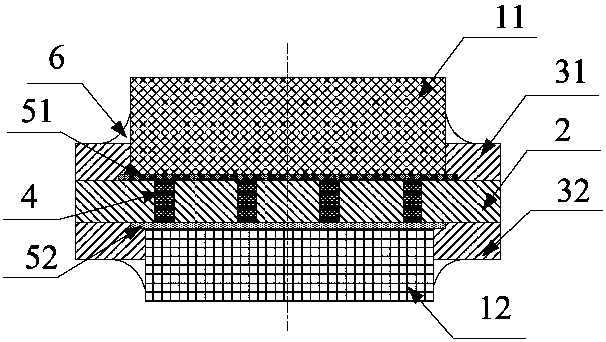
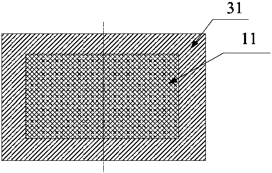
[0024] Such as figure 1 As shown, a bidirectional voltage-resistant silicon carbide solid-state switch includes a silicon carbide chip, an adapter plate 2, a positioning plate, a bonding layer and an insulating passivation layer 6, wherein: the silicon carbide chip includes a silicon carbide upper chip 11 and a silicon carbide The lower chip 12, the middle of the adapter plate 2 is embedded with several interconnected metal columns 4 that run through the adapter plate 2 longitudinally, the positioning plate includes an upper positioning plate 31 and a lower positioning plate 32, and the bonding layer includes an upper bonding layer 51 and The lower bonding layer 52; the upper positioning plate 31 is used to fix the silicon carbide upper chip 11 on the upper bonding layer 51, and the lower positioning plate 32 is used to fix the silicon carbide lower chip 12 on the lower bonding layer 52; The upper chip 11 and the upper positioning plate 31 are connected to the upper surface of...

Embodiment 2

[0033] This embodiment is based on the composition structure of embodiment 1, differs in material:

[0034] The silicon carbide-on-chip 11 is a silicon carbide P-type insulated gate bipolar transistor chip with a withstand voltage of 5000V, an on-resistance of 200-300mΩ, a chip area of ​​2mm×2mm, and a turn-off voltage of not less than -15V;

[0035] The silicon carbide lower chip 12 is a silicon carbide Schottky barrier diode chip with a withstand voltage of 5000V and a chip area of ​​2mm×2mm; the thickness of the adapter plate 2 is 150um; the upper and lower positioning plates 31 and 32 with a thickness of 150um.

[0036]The forward and reverse withstand voltages of the bidirectional silicon carbide solid-state switch of this embodiment are both 5000V, and can be turned off effectively. The gate turn-off voltage is not less than -15V, and the switch size is not more than 3mm×3mm×1.5mm.


PUM

PropertyMeasurementUnit
thicknessaaaaaaaaaa
electrical resistanceaaaaaaaaaa

Abstract

The invention discloses a bidirectional pressure-resistant silicon carbide solid-state switch, which includes a silicon carbide chip, an adapter plate, a positioning plate, and a bonding layer. Embedded with a number of interconnected metal columns that run through the adapter plate longitudinally, the positioning plate includes an upper positioning plate and a lower positioning plate, and the bonding layer includes an upper bonding layer and a lower bonding layer; the silicon carbide upper chip and the upper positioning plate pass through the upper bonding layer The bonding layer is connected to the upper surface of the transfer board, and the silicon carbide lower chip and the lower positioning board are connected to the lower surface of the transfer board through the lower bonding layer; in the middle of the transfer board, there are several interconnected metal columns that run through the transfer board longitudinally , to achieve electrical interconnection through interconnected metal pillars; the invention can realize the effective turn-off and bidirectional withstand voltage of the switch under the premise of being reliable, effective and simple in process, and its volume is equivalent to that of a common silicon carbide chip, and the commonly used silicon carbide chip is used There are no challenging problems in device and packaging process and processing.

Description

technical field [0001] The invention relates to the technical field of power electronics and power semiconductor devices, in particular to a bidirectional voltage-resistant silicon carbide solid-state switch. Background technique [0002] High-voltage, high-current, radiation-resistant, and chip-based semiconductor solid-state switches have great application space in aerospace, power electronics, and power semiconductors. The performance of traditional silicon-based solid-state switches has approached the material limit, making it difficult to improve further. The wide-bandgap semiconductor silicon carbide material has a bandgap width three times that of silicon, and a breakdown field strength that is more than an order of magnitude higher than that of silicon, which can greatly improve the withstand voltage, high current resistance, radiation resistance, and miniaturization and integration level of solid-state switches. [0003] The existing silicon carbide solid-state swi...

Claims


Application Information

Patent Timeline
Patent Type & Authority Patents(China)
IPC IPC(8): H01L25/07H01L23/48
Inventor 代刚张健李俊焘徐星亮张林肖承全周阳
Owner INST OF ELECTRONICS ENG CHINA ACAD OF ENG PHYSICS
Learn More