Array substrate and display device

A technology of array substrate and display area, applied in nonlinear optics, instruments, optics, etc., can solve problems such as signal delay difference on fan-out traces

Inactive Publication Date: 2015-12-30
CHONGQING BOE OPTOELECTRONICS +1
View PDF3 Cites 61 Cited by
  • Summary
  • Abstract
  • Description
  • Claims
  • Application Information

AI Technical Summary

Problems solved by technology

[0003] Embodiments of the present invention provide an array substrate and a display device, which are used to solve the problem of differences in signal delays on fan-out routings existing in the prior art on the basis of ensuring narrow borders

Method used


Image

  • Array substrate and display device
  • Array substrate and display device
  • Array substrate and display device

Examples


Embodiment Construction

[0038] In order to make the purpose, technical solutions and advantages of the present invention clearer, the present invention will be further described in detail below in conjunction with the accompanying drawings. Obviously, the described embodiments are only some of the embodiments of the present invention, rather than all of them. Based on the embodiments of the present invention, all other embodiments obtained by persons of ordinary skill in the art without making creative efforts belong to the protection scope of the present invention.

[0039] The technical solution involved in the present invention will be described in detail through specific examples below, and the present invention includes but is not limited to the following examples.

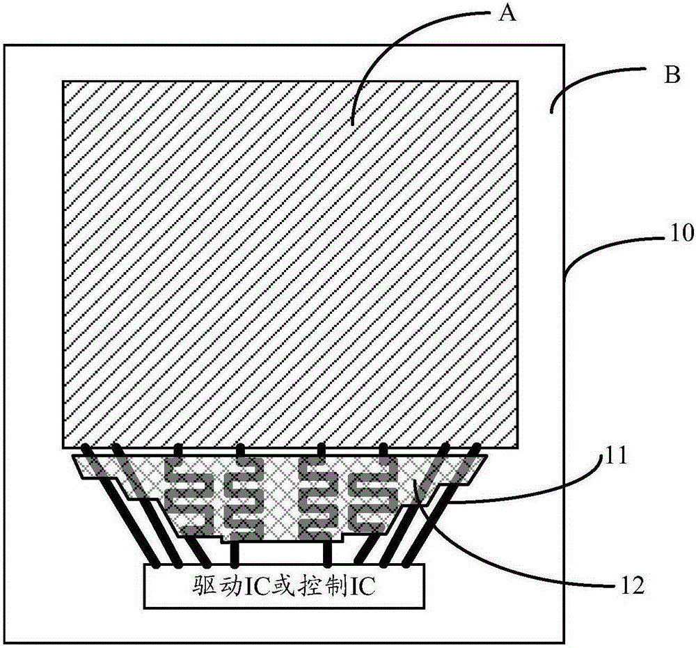
[0040] Such as figure 1 As shown, it is a schematic structural diagram of an array substrate provided by an embodiment of the present invention. The array substrate 10 is limited to a display area A (the middle area of ​​the array s...


PUM


Abstract

The invention discloses an array substrate and a display device. A capacitance compensation film layer is arranged in a non-display region of the array substrate, wherein the capacitance compensation film layer and fanout wires are arranged on different layers. Direct-facing areas between the capacitance compensation film layer and all the fanout wires are gradually increased according to the sequence of length, from big to small, of the fanout wires, the direct-facing areas between the long fanout wires and the capacitance compensation film layer are relatively small, the direct-facing areas between the short fanout wires and the capacitance compensation film layer are relatively big, and then the products of resistance of the long fanout wires and corresponding compensation capacitance are approximately equal to those of resistance of the short fanout wires and corresponding compensation capacitance. Resistance difference can be reduced by means of the design scheme, it is ensured that the products of resistance of all the fanout wires and the corresponding compensation capacitance are approximately equal, the phenomenon that signals of the fanout wires are not uniform is improved, and the uniformity of picture display is promoted. It can be avoided that extra wiring space is additionally arranged, and the narrow-bezel requirement is guaranteed.

Description

technical field [0001] The present invention relates to the field of display technology, in particular to an array substrate and a display device. Background technique [0002] At present, the wiring span of the fanout area (fanout) is relatively large. When wiring from the driver IC to both sides, due to the different positions of the pixel units, the length of each fanout line in the fanout wiring may be different, resulting in a difference in resistance. The signal delay difference on the fan-out traces makes the signal uneven, which in turn affects the uniformity of the screen display; in the prior art, the length of all fan-out traces can be adjusted to be nearly equal by increasing the length of the fan-out traces, thereby reducing the resistance difference, but requires a larger wiring space, which affects the design of narrow borders. Contents of the invention [0003] Embodiments of the present invention provide an array substrate and a display device, which are ...

Claims


Application Information

Patent Timeline
Patent Type & Authority Applications(China)
IPC IPC(8): G02F1/1345G02F1/1362
CPCG02F1/13452G02F1/13458G02F1/1362
Inventor 王小元王武金在光白雅杰
Owner CHONGQING BOE OPTOELECTRONICS
Why Eureka
Try Eureka