Flexible display panel and method for manufacturing same

a flexible display panel and display panel technology, applied in the field of display technology, can solve the problems of increasing manufacturing risks, generating cracks or breaks in this layer, and display panels manufactured by conventional processes have a problem of ir-drop, so as to improve the bending characteristics of flexible display panels, and improve the bending properties

Active Publication Date: 2019-08-22
WUHAN CHINA STAR OPTOELECTRONICS SEMICON DISPLAY TECH CO LTD
View PDF7 Cites 24 Cited by
  • Summary
  • Abstract
  • Description
  • Claims
  • Application Information

AI Technical Summary

Benefits of technology

[0025]According to the present disclosure, organic material having excellent bending property is used to form the interlayer dielectric layer, therefore bending characteristics of flexible display panel is improved. In addition, contact holes in display area and deep hole in bending area are formed after formation of the second gate insulation layer. A part of contact holes are formed at the manufacturing process stage of the first source and drain metal layer. Thus, the holes formed at the manufacturing process stage of the second source and drain metal layer can have low hole density. Therefore, the present disclosure not only ensures improvement of bending characteristics of display panels but also ensures high pixels per inch (PPI) of display panels. Moreover, with formation of a two-layered structure of source and drain metal layers, IR-drop is lowered, and display uniformity of panels is increased. Further, the design of two-layered metal wiring structure in bending area can further lower IR-drop and reduce manufacturing risks.

Problems solved by technology

However, it is prone to result in that stress accumulates in the inorganic interlayer dielectric layer during a bending process of displays, and cracks or breaks are generated in this layer.
In addition, display panels manufactured by conventional processes have a problem of IR-drop (which is a phenomenon where voltage decrease or increase occurs in power or ground networks of integrate circuits).
This affects display uniformity of panels, and increases manufacturing risks.

Method used


Image

  • Flexible display panel and method for manufacturing same
  • Flexible display panel and method for manufacturing same
  • Flexible display panel and method for manufacturing same

Examples


Embodiment Construction

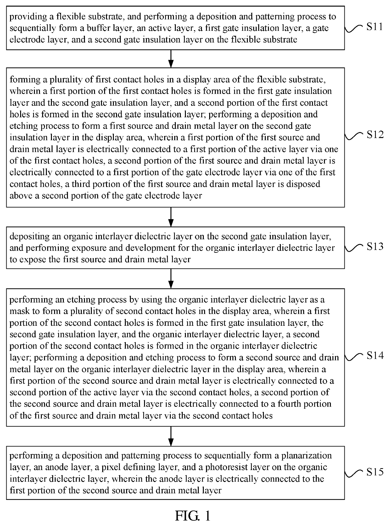
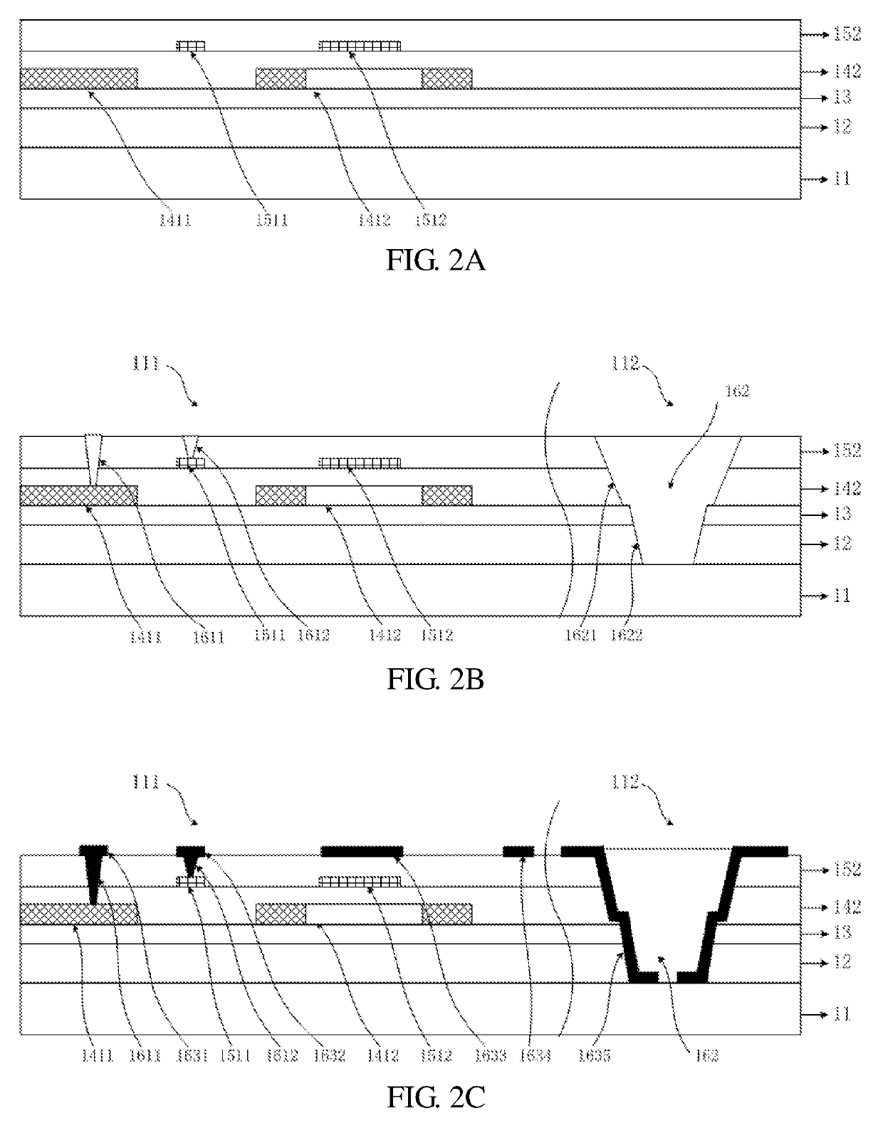
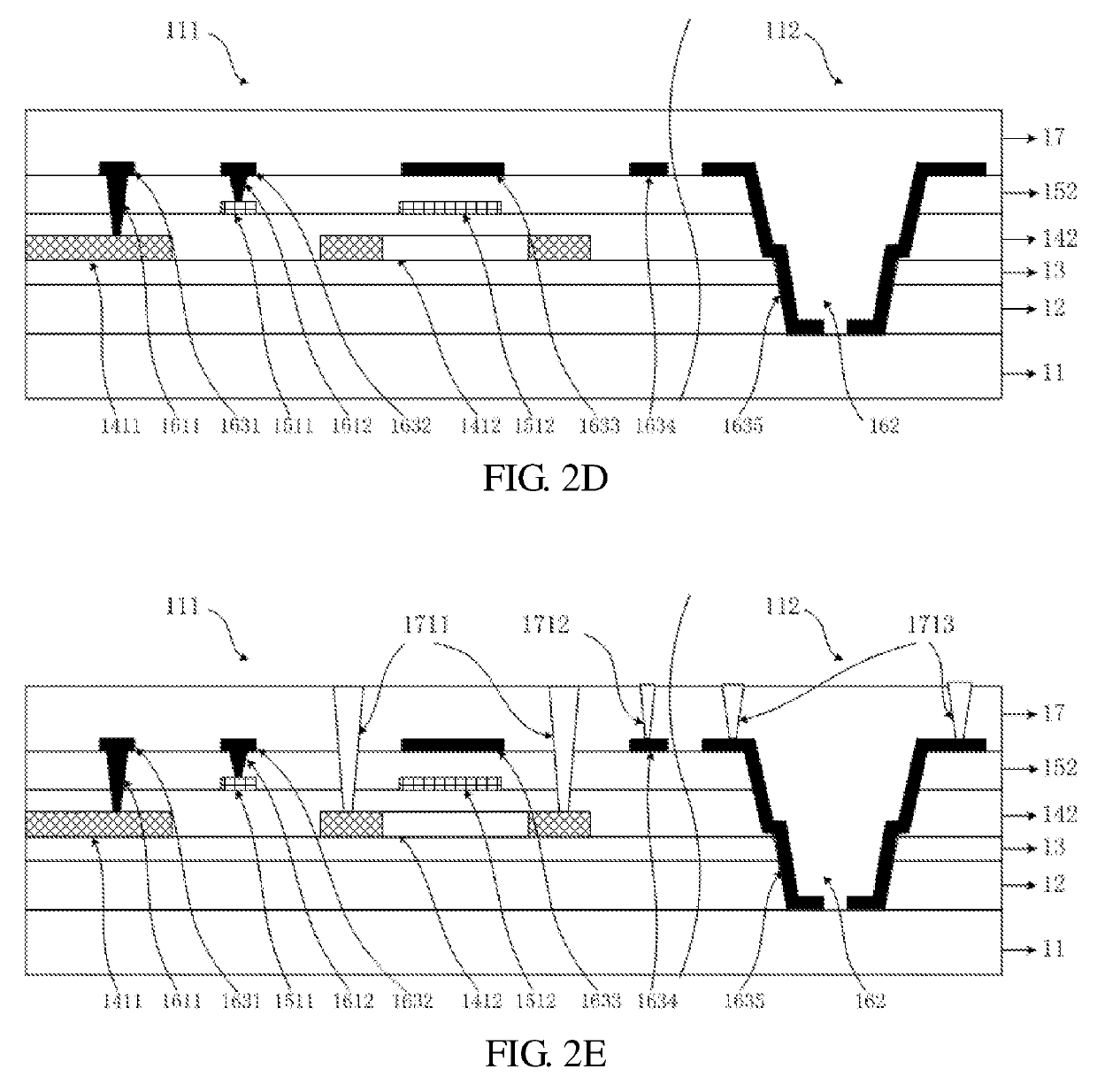
[0030]Reference will be made in detail to embodiments of the present disclosure. The same or similar elements and the elements having same or similar functions are denoted by like reference numerals throughout the descriptions. The embodiments described herein with reference to drawings are explanatory, illustrative, and used to generally understand the present disclosure. The embodiments shall not be construed to limit the present disclosure.

[0031]In the present disclosure, unless specified or limited otherwise, a structure in which a first feature is “on” or “below” a second feature may include an embodiment in which the first feature is in direct contact with the second feature, and may also include an embodiment in which the first feature and the second feature are not in direct contact with each other, but are contacted via an additional feature formed therebetween. Furthermore, a first feature “on,”“above,” or “on top of” a second feature may include an embodiment in which the...


PUM


Abstract

The present disclosure provides a flexible display panel and a method for manufacturing same. The present disclosure not only ensures improvement of bending characteristics of display panels but also ensures high pixels per inch (PPI) of the display panels. Moreover, IR-drop is lowered and display uniformity of the panels is increased.

Description

FIELD OF INVENTION[0001]The present disclosure relates to a field of display technology, and more particularly, to a flexible display panel and a method for manufacturing same.BACKGROUND[0002]Having advantages such as light weight, self-illumination, wide viewing angles, low driving voltage, high light-emitting efficiency, low power consumption, and short response times, organic light-emitting diode (OLED) displays are applied in a variety of products. In particular, because flexible OLED displays are bendable and portable, manufacturers focus their attention on research and development of flexible OLED displays.[0003]In use, flexible displays have to be rolled or flexed, or even bended frequently. According to conventional methods for forming a thin film transistor (TFT) that drives OLED devices, an inorganic interlayer dielectric layer is formed after formation of a second gate electrode layer. However, it is prone to result in that stress accumulates in the inorganic interlayer d...

Claims


Application Information

Patent Timeline
Patent Type & Authority Applications(United States)
IPC IPC(8): H01L51/00G06F1/16H01L51/52H01L27/32
CPCH01L51/0097G06F1/1652H01L51/5206H01L27/3246H01L51/0023G09F9/301H10K59/12H10K59/1213H10K59/131H10K59/1201G09G3/3208G09G2320/0223Y02E10/549H10K59/124H10K77/111H10K2102/311H10K50/81H10K59/122H10K71/621
Inventor YANG, WEIWEI
Owner WUHAN CHINA STAR OPTOELECTRONICS SEMICON DISPLAY TECH CO LTD
Why Eureka
Try Eureka