Method and system for marking special processing patterns in optical proximity effect correction
A technology of optical proximity effect and special processing, which is applied in the direction of photo-plate making process of the original, optics, and pattern surface for photomechanical processing, and can solve problems such as area recognition errors, increase the burden, and avoid recognition errors. Effect
- Summary
- Abstract
- Description
- Claims
- Application Information
AI Technical Summary
Problems solved by technology
Method used
Image

Examples
Embodiment Construction
[0022] In order to make the object, technical solution and advantages of the present invention clearer, the present invention will be further described in detail below in conjunction with the accompanying drawings and embodiments. It should be understood that the specific embodiments described here are only used to explain the present invention, not to limit the present invention.
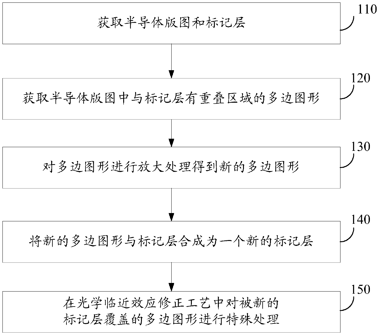
[0023] figure 1 Shown is a method for marking special processing graphics in optical proximity correction in an embodiment, including the following steps.
[0024] S110, acquiring a semiconductor layout and a marking layer.
[0025] In the semiconductor layout, when there is a region that needs to be specially designed, in order to realize the optical proximity correction (OPC), the region is specially treated, and the special region is often marked by adding a marking layer. Due to different requirements of different customers, the marking layer is generally provided by customers. However, the...
PUM
 Abstract
Description
Claims
Application Information
 - R&D Engineer
- R&D Manager
- IP Professional
- Industry Leading Data Capabilities
- Powerful AI technology
- Patent DNA Extraction
Browse by: Latest US Patents, China's latest patents, Technical Efficacy Thesaurus, Application Domain, Technology Topic.
© 2024 PatSnap. All rights reserved.Legal|Privacy policy|Modern Slavery Act Transparency Statement|Sitemap