A method for testing the emission wavelength of Gaas-based semiconductor laser epitaxial wafers and its application
A light-emitting wavelength, semiconductor technology, applied in the direction of measuring optics, instruments, measuring devices, etc., can solve the problems of not being able to make devices, destroying the surface contact layer of epitaxial wafers, etc.
- Summary
- Abstract
- Description
- Claims
- Application Information
AI Technical Summary
Problems solved by technology
Method used
Image

Examples
Embodiment 1
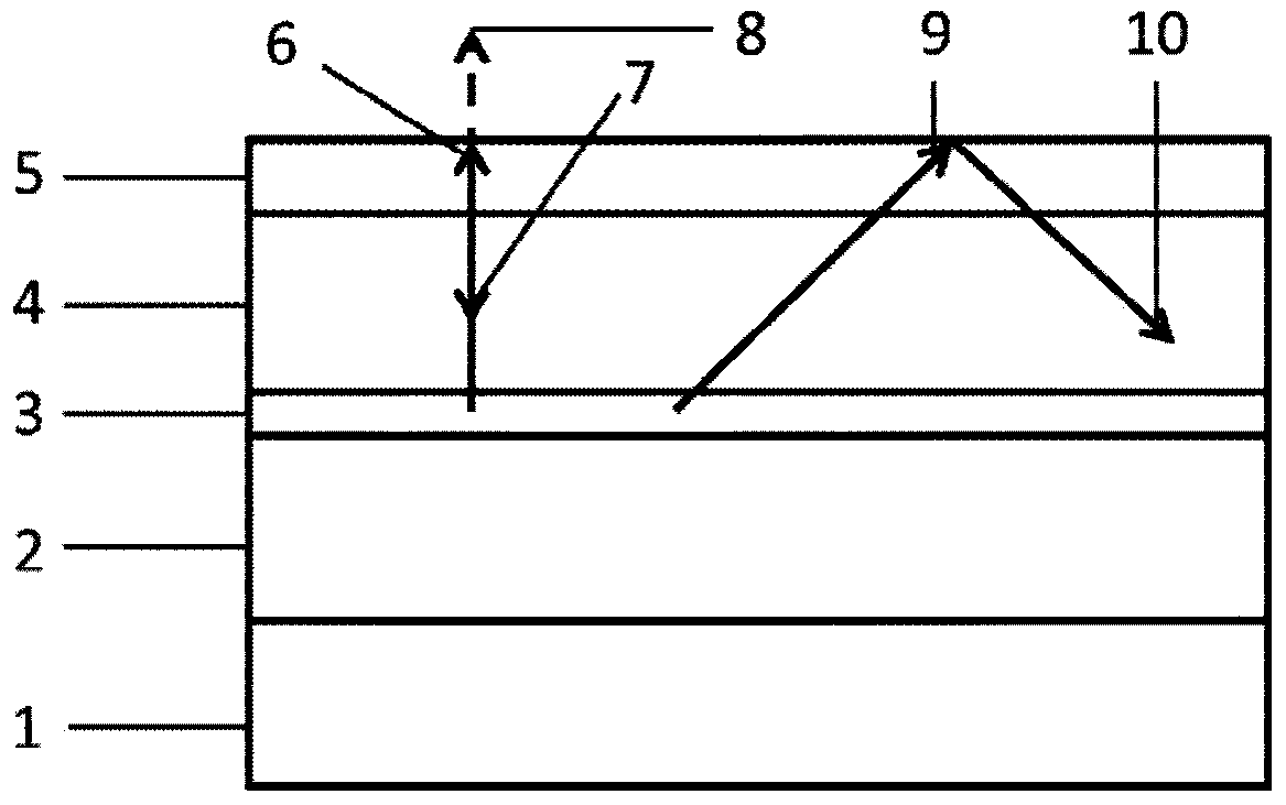
[0043] A method for testing the emission wavelength of a GaAs-based semiconductor laser epitaxial wafer, the GaAs-based semiconductor laser epitaxial wafer includes a substrate 1, a lower cladding layer 2, an active region 3, an upper cladding layer 4, and a contact layer arranged in sequence from bottom to top 5. The substrate 1 is a GaAs single wafer suitable for epitaxial growth, and the lower cladding layer 2 and the upper cladding layer 4 are both Al 0.5 Ga 0.5 As, the active region 3 is a light-emitting region, the contact layer 5 is heavily doped GaAs, the light-emitting wavelength of the GaAs-based semiconductor laser epitaxial wafer is located near 800nm, the structure and light of the GaAs-based semiconductor laser epitaxial wafer of the present invention The output diagram is as figure 1 As shown, the specific steps include:
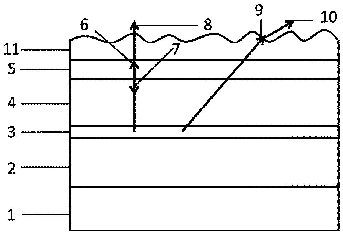
[0044] (1) grow a layer of dielectric film 11 that does not absorb the light emitted by the active region 3 on the surface of the GaAs-base...
Embodiment 2
[0050] A method for testing the emission wavelength of a GaAs-based semiconductor laser epitaxial wafer, the GaAs-based semiconductor laser epitaxial wafer includes a substrate 1, a lower cladding layer 2, an active region 3, an upper cladding layer 4, and a contact layer arranged in sequence from bottom to top 5. The substrate 1 is a GaAs single wafer suitable for epitaxial growth, and the lower cladding layer 2 and the upper cladding layer 4 are both Al 0.5 In 0.5 P, the active region 3 is a light-emitting region, the contact layer 5 is heavily doped GaAs, the light emission wavelength of the GaAs-based semiconductor laser epitaxial wafer is located near 660nm, the structure and light of the GaAs-based semiconductor laser epitaxial wafer of the present invention The output diagram is as figure 1 As shown, the specific steps include:
[0051] (1) grow a layer of dielectric film 11 that does not absorb the light emitted by the active region 3 on the surface of the GaAs-based...
Embodiment 3
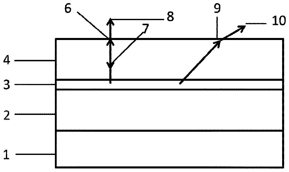
[0057] A GaAs-based semiconductor laser epitaxial wafer for testing the emission wavelength, the GaAs-based semiconductor laser epitaxial wafer includes a substrate 1, a lower cladding layer 2, an active region 3, an upper cladding layer 4, and a contact layer arranged in sequence from bottom to top. Layer 5, the substrate 1 is a GaAs single wafer suitable for epitaxial growth, the lower cladding layer 2 and the upper cladding layer 4 are both Al 0.5 Ga 0.5 As, the active region 3 is a light-emitting region, the contact layer 5 is heavily doped GaAs, the light-emitting wavelength of the GaAs-based semiconductor laser epitaxial wafer is located near 800nm, and the surface of the contact layer 5 is provided with a layer of non-absorbing active region 3 the dielectric film 11 of the emitted light, the value of the refractive index m of the dielectric film 11 is 1.45; the refractive index of the light emitted by the GaAs-based semiconductor laser epitaxial wafer in GaAs is 3.68, a...
PUM
 Abstract
Description
Claims
Application Information
 - R&D
- Intellectual Property
- Life Sciences
- Materials
- Tech Scout
- Unparalleled Data Quality
- Higher Quality Content
- 60% Fewer Hallucinations
Browse by: Latest US Patents, China's latest patents, Technical Efficacy Thesaurus, Application Domain, Technology Topic, Popular Technical Reports.
© 2025 PatSnap. All rights reserved.Legal|Privacy policy|Modern Slavery Act Transparency Statement|Sitemap|About US| Contact US: help@patsnap.com