
Display device and driving method thereof

A display device and display area technology, which is applied to static indicators, instruments, diodes, etc., can solve the problems of low light transmittance, excessive pixel density difference, and overall screen display effects in the optical component setting area, and achieve optimal display effects , reduce differences, improve the effect of impact

Active Publication Date: 2022-07-22
WUHAN TIANMA MICRO ELECTRONICS CO LTD
View PDF5 Cites 0 Cited by
  • Summary
  • Abstract
  • Description
  • Claims
  • Application Information

AI Technical Summary

Problems solved by technology

However, with this setting method, if you want to increase the light transmittance of the optical component setting area to a greater extent, you can only set the pixel density in the optical component setting area to be very small, which leads to the difference between the optical component setting area and the conventional display. The difference in pixel density in the optical component area is too large, which will cause the optical component setting area to affect the display of the overall screen; if you want to reduce the impact of the optical component setting area on the display, the pixel density in the optical component setting area cannot be too small, which will lead to The light transmittance of the optical component setting area is low, which affects the imaging effect

Method used


Image

  • Display device and driving method thereof
  • Display device and driving method thereof
  • Display device and driving method thereof

Examples


Embodiment Construction

[0032] In order to better understand the technical solutions of the present invention, the embodiments of the present invention are described in detail below with reference to the accompanying drawings.

[0033] It should be understood that the described embodiments are only some, but not all, embodiments of the present invention. Based on the embodiments of the present invention, all other embodiments obtained by those of ordinary skill in the art without creative efforts shall fall within the protection scope of the present invention.

[0034] The terms used in the embodiments of the present invention are only for the purpose of describing specific embodiments, and are not intended to limit the present invention. As used in the embodiments of the present invention and the appended claims, the singular forms "a," "the," and "the" are intended to include the plural forms as well, unless the context clearly dictates otherwise.

[0035] It should be understood that the term "an...


PUM


Abstract

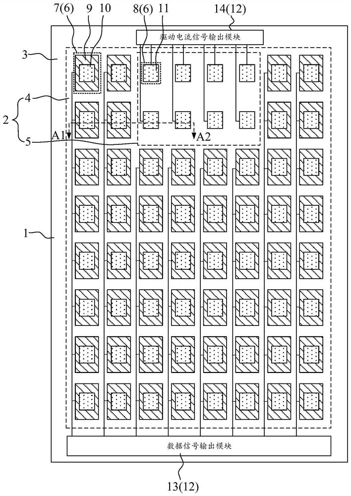
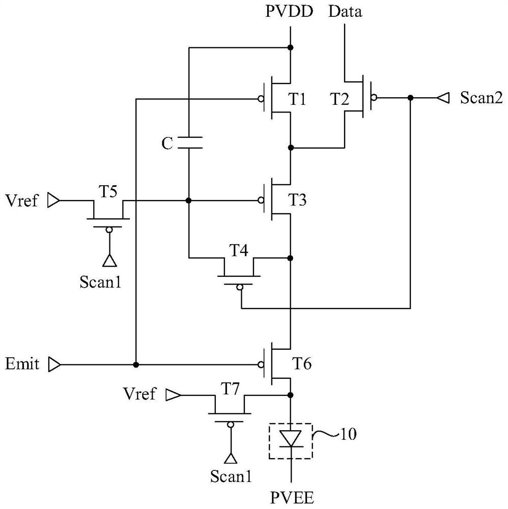
Embodiments of the present invention provide a display device and a driving method thereof, which relate to the field of display technology, improve the light transmittance of an optical component setting area, and improve the influence of the optical component setting area on display. The display device includes a display panel, and the display panel includes: a display area including a first display area and an optical component setting area; and a sub-pixel including a first sub-pixel located in the first display area and a first sub-pixel located in the optical component setting area. Two sub-pixels; the first sub-pixel includes a first pixel circuit and a first light-emitting element, and the second sub-pixel includes a second light-emitting element; it also includes a driving chip, and the driving chip includes: a data signal output module, which is electrically connected to the first pixel circuit , for outputting the first data signal to the first pixel circuit, so that the first pixel circuit drives the first light-emitting element to emit light; the driving current signal output module, which is electrically connected to the second light-emitting element, is used for outputting the second light-emitting element to the second light-emitting element. The driving current signal drives the second light-emitting element to emit light.

Description

【Technical field】 [0001] The present invention relates to the field of display technology, and in particular, to a display device and a driving method thereof. 【Background technique】 [0002] A display device with a camera function includes a display panel and a camera, wherein the display panel is provided with an optical component setting area, and the optical component setting area corresponds to the setting position of the camera. At present, the number of metal wires in the optical component setting area is usually reduced by reducing the pixel density in the optical component setting area, thereby improving the light transmittance of the optical component setting area. However, with this setting method, if the light transmittance of the optical component setting area is to be improved to a greater extent, the pixel density of the optical component setting area can only be set to a small value, which leads to the difference between the optical component setting area and...

Claims


Application Information

Patent Timeline
Patent Type & Authority Patents(China)
IPC IPC(8): G09G3/20
CPCG09G3/2074G09G2300/0426G09G2310/0286G09G3/3266G09G3/3275H01L27/156H10K59/65H10K59/123H10K59/131G09G3/32G09G2310/027H01L31/125H01L33/24
Inventor 何雨谦
Owner WUHAN TIANMA MICRO ELECTRONICS CO LTD
Learn More