A kind of LED chip electrode and manufacturing method thereof

A technology of LED chip and manufacturing method, which is applied in the direction of circuits, electrical components, semiconductor devices, etc., can solve the problems of voltage rise, affecting luminous efficiency, and easy detachment of electrodes, etc., to achieve improved luminous efficiency, increased emission rate, and high brightness Effect

Active Publication Date: 2017-10-10
XIANGNENG HUALEI OPTOELECTRONICS
View PDF5 Cites 0 Cited by
  • Summary
  • Abstract
  • Description
  • Claims
  • Application Information

AI Technical Summary

Problems solved by technology

The Al layer is directly in contact with the surface of the GaN epitaxial layer. Although the luminous efficiency of the LED can be guaranteed, there are two problems: one is that the adhesion between the entire electrode and GaN will be poor, and the electrode will be damaged during the subsequent wire bonding and bonding process. Easy to fall off; Second, the voltage will increase
In the existing electrode structure, a metal thin film, such as a chromium layer, is designed between the aluminum layer and the surface of the GaN epitaxial layer, which can not only ensure the adhesion of the electrode, but also reduce the voltage, but this thin film will generate light. Absorption, which affects the luminous efficiency of the LED

Method used


Image

  • A kind of LED chip electrode and manufacturing method thereof
  • A kind of LED chip electrode and manufacturing method thereof
  • A kind of LED chip electrode and manufacturing method thereof

Examples


Embodiment 1

[0033] combine Figure 2-Figure 9 , the present embodiment provides a method for manufacturing an electrode of an LED chip, comprising the steps of:

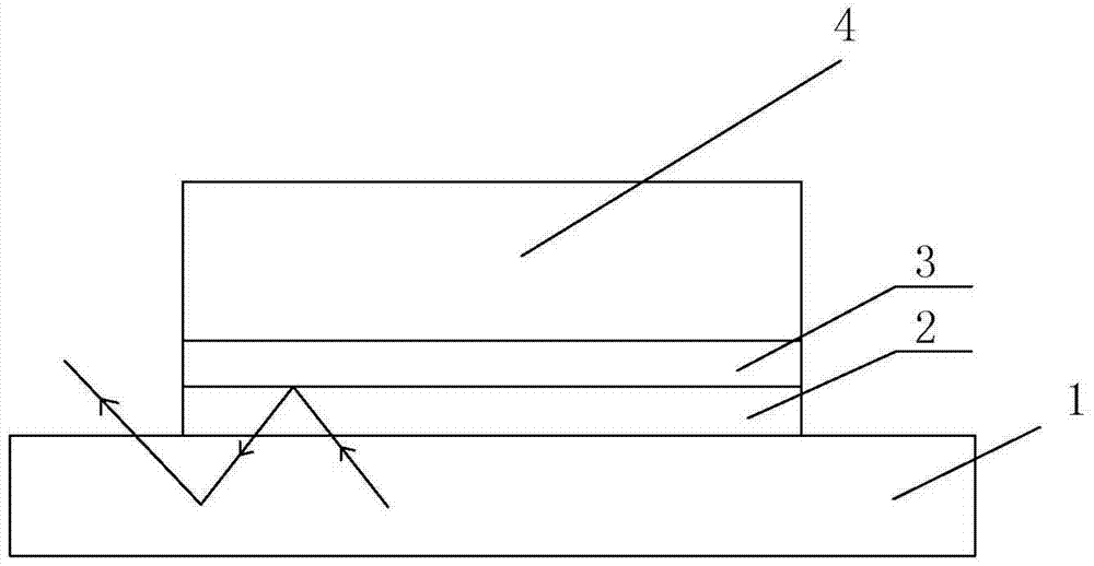
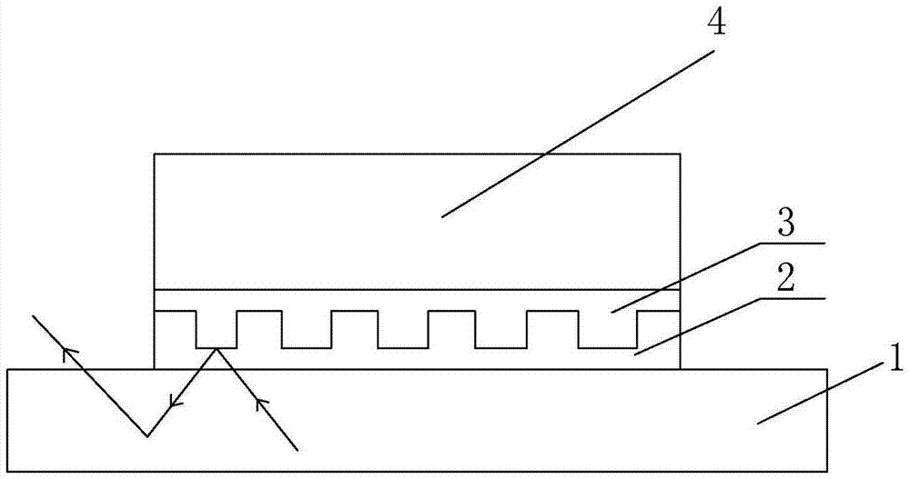
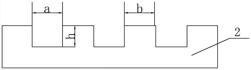
[0034] Step 101: The dry etching equipment ICP etches the epitaxial layer 1 including the N-type GaN layer, the quantum well and the P-type GaN layer from bottom to top, forming steps to expose the N-type GaN layer, with an etching depth of 1 μm, and cutting lines The width is between 10 μm, the P electrode is made on the P-type GaN layer, and the N electrode is made on the N-type GaN layer;

[0035] Step 102: Electron beam vacuum evaporation method is used to make the conductive layer of indium tin oxide film, and the film thickness is , chamber temperature 150°C, oxygen flow rate 5sccm, vacuum degree 3×10 -5 Torr;

[0036] Step 103: if Figure 4 As shown, a negative photoresist 5 with a thickness of 2.5 μm is coated, exposed and developed to expose the electrode region;

[0037] Step 104: if Figure 5 As shown, the elec...

Embodiment 2

[0046] to combine Figure 2-Figure 9 , the present embodiment provides a method for manufacturing an electrode of an LED chip, comprising the steps of:

[0047] Step 201: The dry etching equipment ICP etches the epitaxial layer 1 including the N-type GaN layer, the quantum well and the P-type GaN layer from bottom to top, forming steps to expose the N-type GaN layer, with an etching depth of 2 μm, and cutting lines The width is between 25 μm, the P electrode is made on the P-type GaN layer, and the N electrode is made on the N-type GaN layer;

[0048] Step 202: Electron beam vacuum evaporation method is used to make the conductive layer of indium tin oxide film, and the film thickness is , chamber temperature 350°C, oxygen flow rate 15sccm, vacuum degree 3×10 -7 Torr;

[0049] Step 203: if Figure 4 As shown, a negative photoresist 5 with a thickness of 3.0 μm is coated, exposed and developed to expose the electrode region;

[0050] Step 204: if Figure 5 As shown, the ...

Embodiment 3

[0059] to combine Figure 2-Figure 9 , the present embodiment provides a method for manufacturing an electrode of an LED chip, comprising the steps of:

[0060] Step 301: The dry etching equipment ICP etches the epitaxial layer 1 including the N-type GaN layer, the quantum well and the P-type GaN layer from bottom to top in order to form steps to expose the N-type GaN layer, the etching depth is 1.5 μm, and the cutting line The width is between 17 μm, the P electrode is made on the P-type GaN layer, and the N electrode is made on the N-type GaN layer;

[0061] Step 302: making an indium tin oxide thin film conductive layer by electron beam vacuum evaporation method, the film thickness is The chamber temperature is 250°C, the oxygen flow rate is 10sccm, and the vacuum degree is 5.05×10 -6 Torr;

[0062] Step 303: if Figure 4 As shown, a negative photoresist 5 with a thickness of 2.7 μm is coated, exposed and developed to expose the electrode region;

[0063] Step 304: if...


PUM


Abstract

The invention discloses a fabrication method of an LED chip electrode. The fabrication method includes the following steps that: dry etching is performed on an epitaxial layer, an N type GaN layer is exposed; an indium tin oxide film conductive layer is fabricated; a chromium layer is formed through evaporation; a nickel layer is formed through evaporation; annealing treatment is performed on the nickel layer under a nitrogen atmosphere, so that the nickel layer can form uniformly-distributed spherical nickel particles on the surface of the chromium layer; with the spherical nickel particles adopted as an etching mask, the chromium layer is etched, so that nanoscale recessed rectangular pits can be formed on the surface of the chromium layer through etching; the spherical nickel particles are removed through corrosion; an aluminized layer, a titanium layer, a platinum layer and a gold layer are formed sequentially through evaporation; and glue is removed through peeling, and as a result, the LED chip electrode can be obtained. The invention also discloses an LED chip electrode; the LED chip electrode includes a chromium layer, an aluminum layer, an evaporation aluminum, a titanium layer, a platinum layer and a gold layer which are distributed sequentially from bottom to top; and nanoscale recessed rectangular pits can be formed on the surface of the chromium layer through etching. According to the LED chip electrode and the fabrication method thereof of the invention, the nanoscale lumpy structures can be formed on the surface of the chromium layer, so that the exitance of light on the surface of the chromium layer can be increased; light that is reflected into the chip by the aluminum layer and is further reflected out can be increased, and therefore, the luminous efficiency of an LED can be obviously improved.

Description

technical field [0001] The invention relates to the field of optoelectronic devices, in particular to an LED chip electrode and a manufacturing method thereof. Background technique [0002] LED is a solid light source, which is a light-emitting device made of semiconductor P-N junction. During forward conduction, the minority carriers in the semiconductor recombine with the majority carriers, and the released energy is emitted in the form of photons or partly in the form of photons. Semiconductor LED lighting has significant advantages such as high efficiency, energy saving, environmental protection, long service life, etc., and has been widely used in various fields such as street lamps, display screens, indoor lighting, and automobile lights. How to improve luminous efficiency is the main problem that LED needs to solve. [0003] At present, most LED electrodes use a reflective electrode structure containing an aluminum layer. The aluminum layer in the electrode can refl...

Claims


Application Information

Patent Timeline
Patent Type & Authority Patents(China)
IPC IPC(8): H01L33/40H01L33/38
CPCH01L33/38H01L33/40H01L33/405H01L2933/0016
Inventor 徐平苗振林卢国军周佐华
Owner XIANGNENG HUALEI OPTOELECTRONICS
Why Eureka
Try Eureka