Check patentability & draft patents in minutes with Patsnap Eureka AI!

Alignment detection method for multi-layer circuit board

A technology of multi-layer circuit and detection method, applied in the direction of multi-layer circuit manufacturing, measuring device, printed circuit, etc., can solve the problem of difficult detection and other problems

Active Publication Date: 2018-09-11
KALEX MULTI LAYER CIRCUIT BOARD (ZHONGSHAN) CO LTD
View PDF3 Cites 0 Cited by
  • Summary
  • Abstract
  • Description
  • Claims
  • Application Information

AI Technical Summary

Problems solved by technology

[0004] Based on this, it is necessary to provide a multilayer circuit board alignment detection method that can easily detect the interlayer alignment for the problem that the interlayer alignment detection of multilayer circuit boards is difficult

Method used


Image

  • Alignment detection method for multi-layer circuit board
  • Alignment detection method for multi-layer circuit board
  • Alignment detection method for multi-layer circuit board

Examples


Embodiment Construction

[0035] In order to facilitate the understanding of the present invention, the present invention will be described more fully below with reference to the associated drawings. Preferred embodiments of the invention are shown in the accompanying drawings. However, the present invention can be embodied in many different forms and is not limited to the embodiments described herein. On the contrary, these embodiments are provided to make the understanding of the disclosure of the present invention more thorough and comprehensive.

[0036] It should be noted that when an element is referred to as being “fixed” to another element, it can be directly on the other element or there can also be an intervening element. When an element is referred to as being "connected to" another element, it can be directly connected to the other element or intervening elements may also be present. The terms "vertical," "horizontal," "left," "right," and similar expressions are used herein for purposes ...


PUM


Abstract

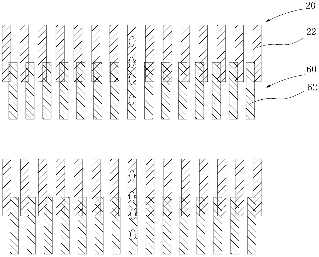
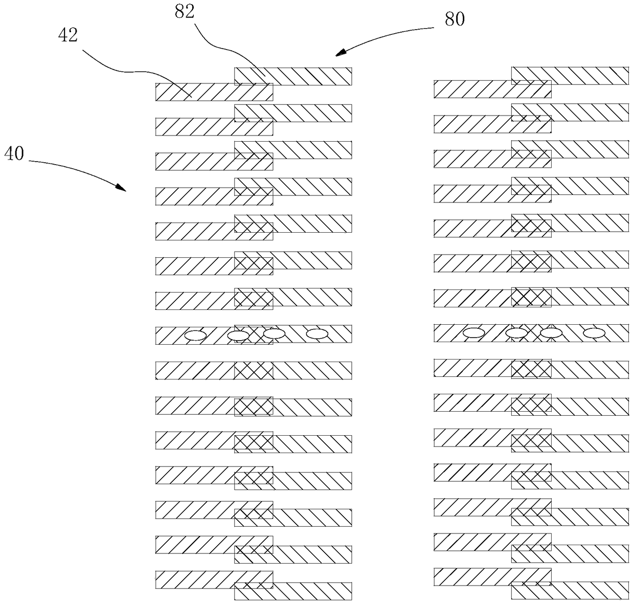
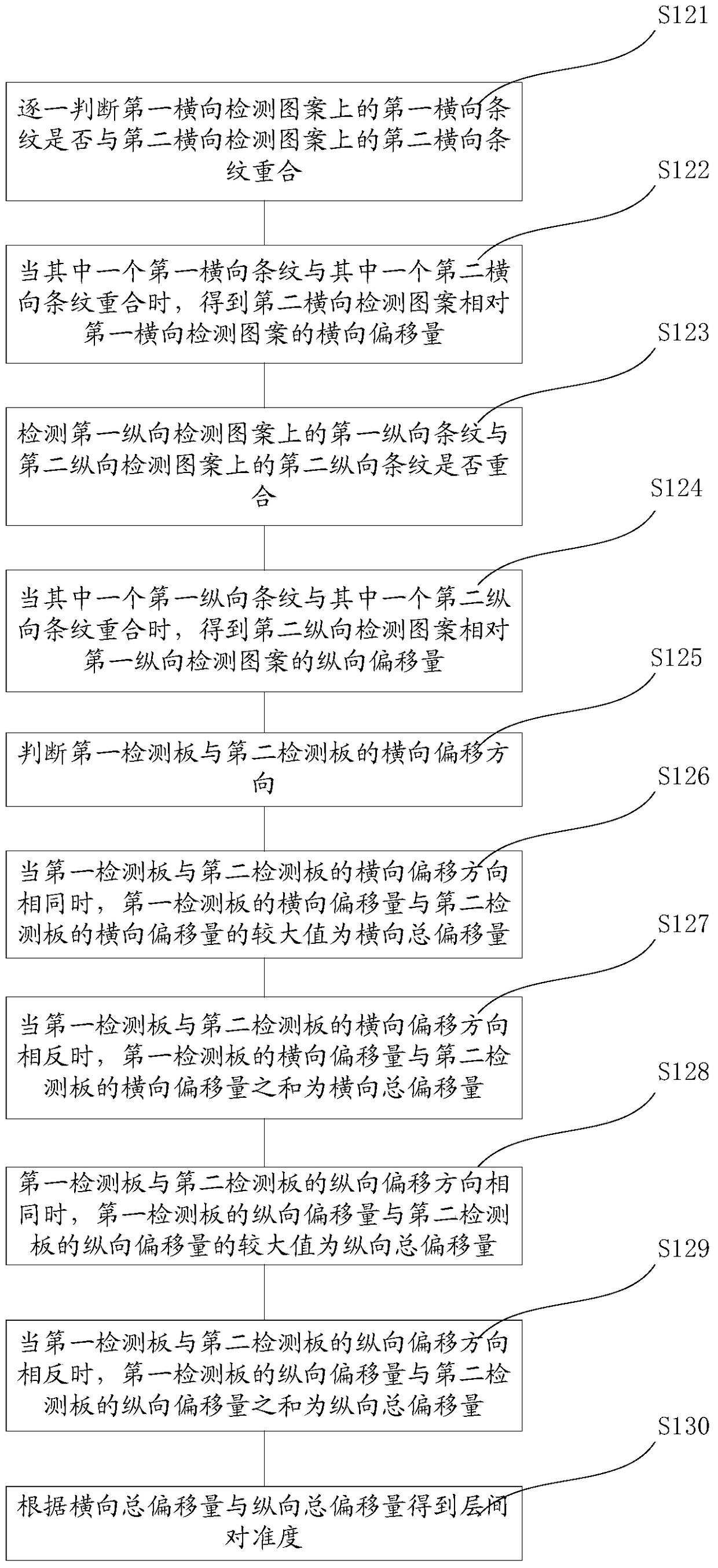
The invention relates to a multilayer circuit board alignment degree detection method, which is used for detecting the alignment degree of a multilayer circuit board. The multilayer circuit board comprises a plurality of circuit boards which are arranged in a stacked mode. The multilayer circuit board alignment degree detection method comprises the steps of setting one of the plurality of circuit boards to be a reference board, wherein the reference board is provided with a first detection pattern, and setting another one of the plurality of circuit boards to be a detection board, wherein the detection board is provided with a second detection pattern; and detecting an offset of the second detection pattern on the detection board relative to the first detection pattern on the reference board by using X-rays so as to acquire the interlayer alignment degree. According to the multilayer circuit board alignment degree detection method, the offset of the first detection pattern relative to the second detection pattern can be acquired through directly detecting the partially overlapped first detection pattern and the second detection pattern which are correspondingly arranged on the reference board and the detection board in a stacked mode through the X-rays, so that the interlayer alignment degree is acquired, and operations such as slicing are not required to be carried out on the multilayer circuit board, thereby shortening the detection time, and having high detection efficiency.

Description

technical field [0001] The invention relates to the field of detection of interlayer alignment of printed circuit boards, in particular to a method for detection of alignment of multilayer circuit boards. Background technique [0002] With the development of society and the advancement of technology, the packaging density of integrated circuits has gradually increased, resulting in a high concentration of interconnection lines, which has led to the increasing use of multilayer circuit boards. At present, Mass Lam (pinless positioning lamination process) is usually used to make multi-layer boards with n layers from L1 to Ln. The method is as follows: first make L2 / L3, L4 / L5,...Ln-2 / Ln-1 multiple For each inner layer core board, multiple inner layer core boards are fused and fixed with corresponding specifications and quantities of prepregs, and then a MassLam press is used to apply a certain temperature and pressure to cure the multilayer board. The multi-layer board produce...

Claims


Application Information

Patent Timeline
Patent Type & Authority Patents(China)
IPC IPC(8): H05K3/46G01B15/00
CPCG01B15/00H05K3/4638H05K2203/166
Inventor 戴匡
Owner KALEX MULTI LAYER CIRCUIT BOARD (ZHONGSHAN) CO LTD
Features
  • R&D
  • Intellectual Property
  • Life Sciences
  • Materials
  • Tech Scout
  • Unparalleled Data Quality
  • Higher Quality Content
  • 60% Fewer Hallucinations
Learn More