Chip testing and sorting method

A chip testing and sorting technology, applied in the direction of measuring electricity, measuring devices, measuring electrical variables, etc., can solve problems such as FAIL, misclassified results, etc.

Inactive Publication Date: 2016-04-06
华润赛美科微电子(深圳)有限公司
View PDF9 Cites 10 Cited by
  • Summary
  • Abstract
  • Description
  • Claims
  • Application Information

AI Technical Summary

Problems solved by technology

If the TEST1 test is passed (PASS), but the TEST2 test is not passed (FAIL), the sorting machine will classify the chips of the first station manipulator 1 into the PASS class, and classify the chips of the second station manipulator 2 into the FAIL class In the middle, but in fact TEST2 is testing the chip on the first station manipulator 1, which will lead to FAIL products in the PASS category
Similarly, if the communication cable is wrongly connected and the test cable connecting the manipulator to the test port is connected correctly, this misclassification result will also be generated.

Method used


Image

  • Chip testing and sorting method
  • Chip testing and sorting method
  • Chip testing and sorting method

Examples


Embodiment Construction

[0030] The specific embodiments of the present invention will be described in detail below in conjunction with the accompanying drawings.

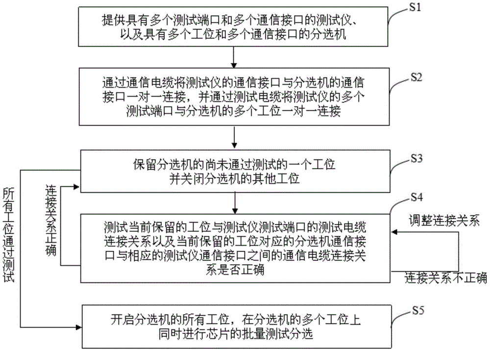
[0031] image 3 It is a flowchart of a chip testing and sorting method provided by the present invention, and the chip testing and sorting method includes the following steps S1-S5.

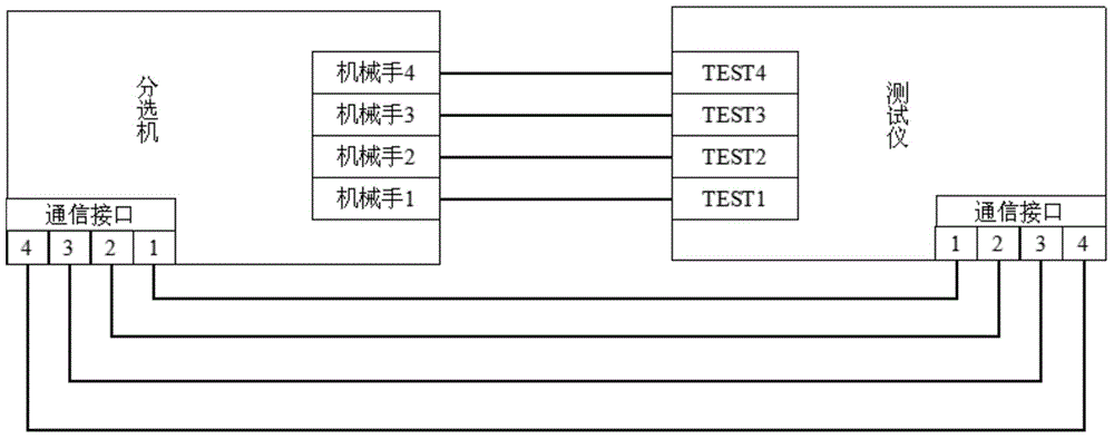
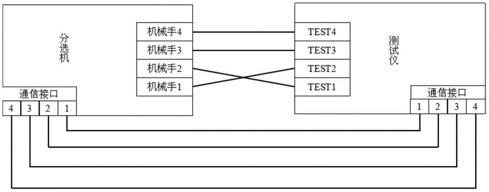
[0032] S1. Provide a tester with multiple test ports and multiple communication interfaces, and a sorter with multiple stations and multiple communication interfaces.

[0033] Please also see Figure 4 , in this embodiment, the tester 10 provided by S1 includes four test ports TEST1, TEST2, TEST3, TEST4 and a plurality of communication interfaces 101, 102, 103, 104; the sorter 20 provided by S1 includes four communication interfaces 201 , 202, 203, 204 and four stations. In this embodiment, each station of the sorter 20 is a manipulator for grabbing the chips to be tested, and the four stations of the sorter 20 are manipulator 1 , manipulator 2 , manipulat...


PUM


Abstract

The present invention relates to a chip testing and sorting method which comprises the steps of (S1) providing a tester and a multi-station sorter, (S2) connecting the tester and the communication interface of the sorter through a cable, and connecting the test port of the tester and the station of the sorter, (S3) reserving a station which does not pass a test of the sorter and closing other stations of the sorter, (S4) testing whether the cable connection relation of the currently reserved station is correct or not, showing that the currently reserved station passes the test if the connection relation is correct, repeating the step (S3) until all stations pass the test, adjusting the cable connection relation of the currently reserved station if the connection relation is wrong, and repeating the step (S4), and (S5) starting all stations of the sorter, and carrying out batch test sorting of chips. According to the chip testing and sorting method, the wrong classification problem caused by the wrong cable connection of multiple stations can be effectively avoided.

Description

technical field [0001] The invention relates to the field of semiconductor device testing, in particular to a multi-station semiconductor packaging chip testing and sorting method. Background technique [0002] With the continuous development of semiconductor manufacturing and testing technology, sorting machines are widely used in the testing process of semiconductor devices to test the quality of semiconductor packaged chips (IC) and sort out qualified and unqualified finished products. As the production capacity of semiconductor packaged chips continues to increase, in order to improve the efficiency of testing and sorting, the sorting machine usually has multiple stations to simultaneously test and sort multiple semiconductor packaged chips. [0003] figure 1 An example is given to illustrate the electrical connection relationship between the existing multi-station sorter and the tester (ATE). The sorting machine includes four communication interfaces 1, 2, 3, 4 and fo...

Claims


Application Information

Patent Timeline
IPC IPC(8): G01R31/01
Inventor 顾汉玉
Owner 华润赛美科微电子(深圳)有限公司
Why Eureka
Try Eureka