A method for layout and wiring of anti-single event reinforced circuit unit
An anti-single event, layout and wiring technology, applied in the direction of electrical digital data processing, special data processing applications, instruments, etc., can solve problems such as difficulties in realizing circuit layout, improve the ability of anti-single event effect, accurate layout positioning, and enhance The effect of anti-radiation hardening effect
- Summary
- Abstract
- Description
- Claims
- Application Information
AI Technical Summary
Problems solved by technology
Method used
Image

Examples
Embodiment Construction
[0031] The working process of the present invention will be further explained below in conjunction with the accompanying drawings.
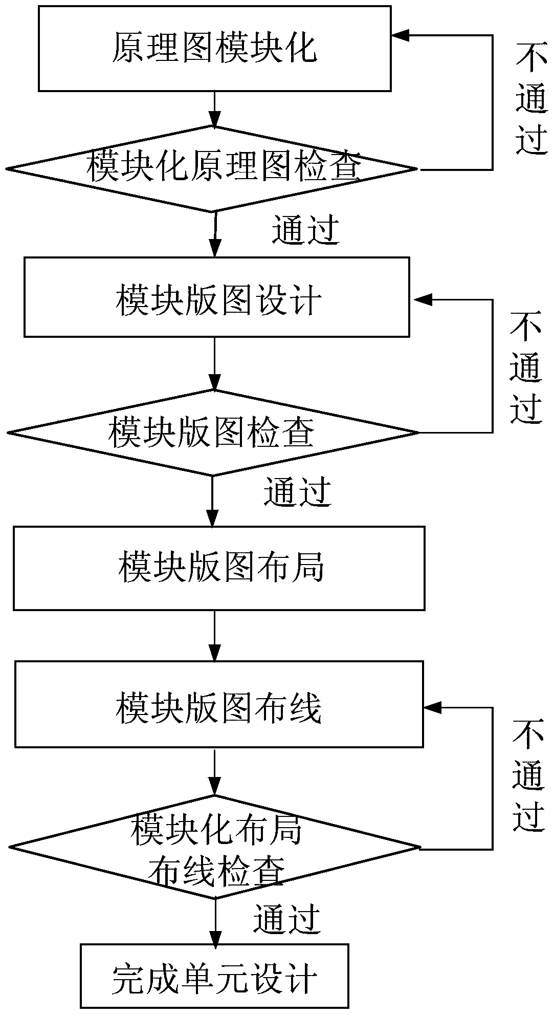
[0032] Such as figure 1 As shown, a method for layout and wiring of an anti-single event reinforced circuit unit includes the following steps:
[0033] (1) Schematic diagram modularization: According to the separation requirements of sensitive nodes in the anti-single event hardened circuit, the schematic diagram of the anti-single event hardened circuit is modularized, that is, split into several modules with input and output ports, and the connections between modules The relationship is consistent with the split circuit;
[0034] The specific implementation of schematic diagram modularization is as follows:
[0035] (a) According to the distribution of sensitive nodes, split the overall circuit into modules greater than or equal to the number of sensitive nodes, and each module can only contain one sensitive node;
[0036] (b) Divide the is...
PUM
 Abstract
Description
Claims
Application Information