

Erasing method of three-dimensional memory device
A three-dimensional storage and device technology, applied in the field of erasing three-dimensional semiconductor memory devices, can solve problems such as device failure, data retention characteristic degradation, and hole residue, and achieve the effect of avoiding device failure.
- Summary
- Abstract
- Description
- Claims
- Application Information
AI Technical Summary
Problems solved by technology
Method used
Image

Examples
Embodiment Construction
[0035] The features and technical effects of the technical solution of the present invention will be described in detail below with reference to the accompanying drawings and in conjunction with exemplary embodiments, and a method for erasing a semiconductor storage device that allows electrons in the storage layer to be completely erased without remaining holes is disclosed. It should be pointed out that similar reference numerals represent similar structures, and the terms "first", "second", "upper", "lower" and the like used in this application can be used to modify various device structures or manufacturing processes . These modifications do not imply spatial, sequential or hierarchical relationships of the modified device structures or fabrication processes unless specifically stated.
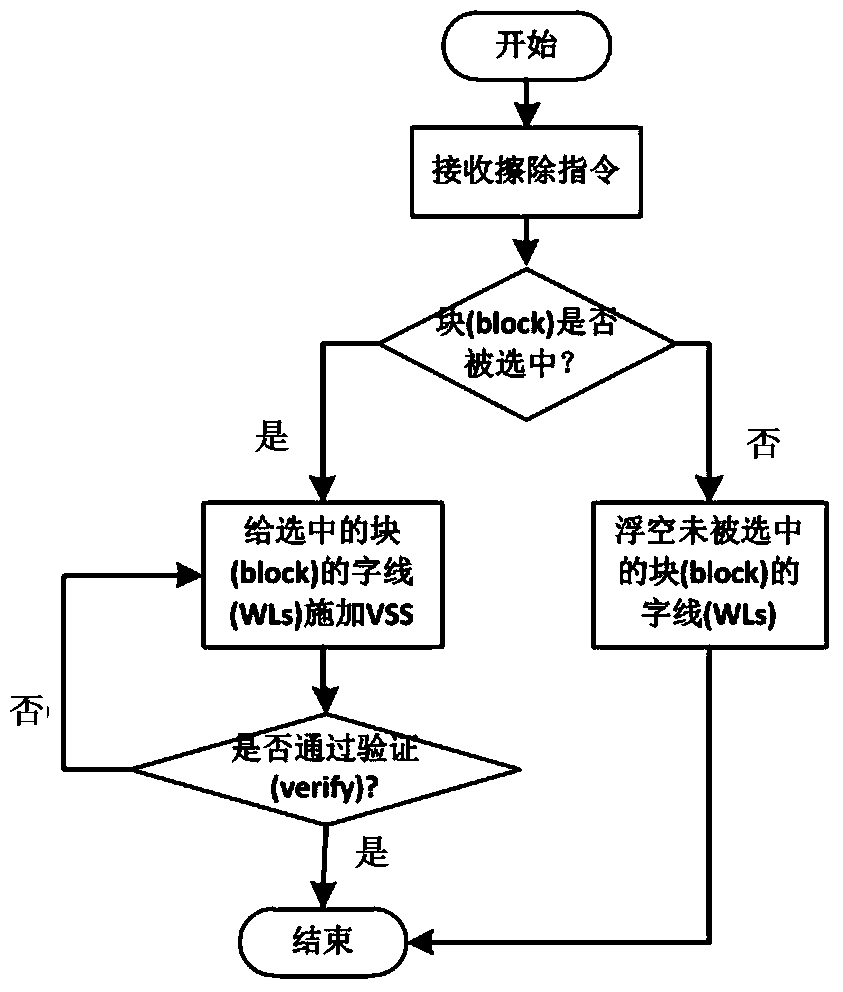
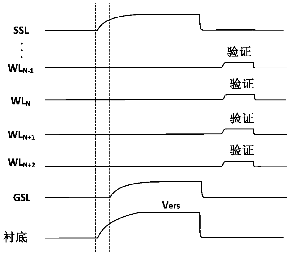
[0036] Such as Figure 5 and Figure 6 As shown, the erasing method of a 3D memory device according to an embodiment of the present invention includes the following steps:
[0037] 1. R...
PUM
 Abstract
Description
Claims
Application Information