Printed wiring board and method of producing the same

A printed circuit board, one-sided technology, applied in the direction of printed circuit manufacturing, printed circuit, printed circuit, etc., can solve the problems that hinder the miniaturization of the unit unit, and achieve the effect of reducing high-frequency noise current

Active Publication Date: 2016-06-08
UNIV OKAYAMA +1
View PDF7 Cites 10 Cited by
  • Summary
  • Abstract
  • Description
  • Claims
  • Application Information

AI Technical Summary

Problems solved by technology

The allowable current value is determined by the thickness of the meandering wiring portion, so when a large current is supplied, the meandering wiring needs to be thickened, which hinders the miniaturization of the unit cell

Method used


Image

  • Printed wiring board and method of producing the same
  • Printed wiring board and method of producing the same
  • Printed wiring board and method of producing the same

Examples


Embodiment Construction

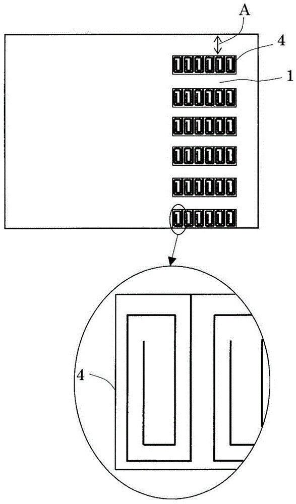
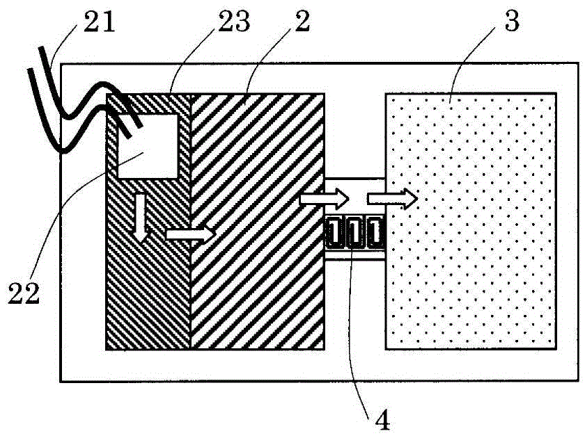
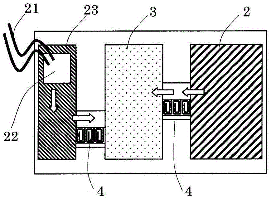
[0025] The printed wiring board according to one embodiment of the present invention will be described based on the drawings. In printed circuit boards, such as figure 1 As shown, the power layer width (width A) of the part connecting the digital power module and the analog power module is a width that satisfies the current value required by the IC (semiconductor integrated circuit), which can be 2-6mm, preferably 3-4mm . There may be one bridge 1 or multiple bridges.

[0026] The shape of the open stub EBG structure 4 formed on the power supply pattern (power supply path) of the printed circuit board, such as figure 1 As shown in the partial enlarged view, it is better to form a vortex with the open part as the center and minimize the occupied area as much as possible. The spiral shape can be bent regardless of whether it is a curve or a straight line, and the position and number of bending are arbitrary in the case of bending. The bending angle is also not limited to a righ...


PUM

PropertyMeasurementUnit
Thicknessaaaaaaaaaa

Abstract

A printed wiring board includes a digital circuit, an analog circuit, and a power supply path that is disposed on an insulating layer between the digital circuit and the analog circuit. A plurality of open stub EBG structures are disposed at an end of a bridge section in a power supply plane. The open stub EBG structure is an open stub state whose one end is connected to the power supply path and other end is in an open state.

Description

Technical field [0001] The invention relates to a printed circuit board with an electromagnetic band gap (EBG) structure and a manufacturing method thereof. Background technique [0002] In recent years, a structure for artificially controlling the dispersion of electromagnetic waves by periodically arranging conductor patches and the like has been proposed. Among them, the electromagnetic band gap (Electromagnetic Band Gap, hereinafter referred to as "EBG") structure has the characteristic of suppressing the propagation of electromagnetic waves in a specific frequency band of the printed circuit board and the device package substrate, and using this characteristic is applied to noise suppression and interference countermeasures Wait. [0003] As the EBG structure, for example, a mushroom-type EBG structure having a mushroom-shaped conductor, a through-hole-free EBG structure without using a through-hole, and the like are proposed. [0004] In the existing multilayer printed wiring...

Claims


Application Information

Patent Timeline
IPC IPC(8): H05K1/02H05K3/00
CPCH05K1/0236H05K3/0011H05K2201/083
Inventor 丰田启孝五百籏头健吾山下祐辉金子俊之内藤政则海谷清彦上原利久近藤幸一
Owner UNIV OKAYAMA
Why Eureka
Try Eureka