
High Electron Mobility Transistor

A technology of charge carriers and semiconductors, applied in circuits, electrical components, semiconductor devices, etc.

Active Publication Date: 2021-06-11
POWER INTEGRATIONS INC
View PDF5 Cites 0 Cited by
  • Summary
  • Abstract
  • Description
  • Claims
  • Application Information

AI Technical Summary

Problems solved by technology

Because the input capacitance of the gate increases as the field plate connected to the gate approaches the drain, it has been introduced that once the saturation length is reached, the extension of the field plate connected to the gate towards the drain is limited

Method used


Image

  • High Electron Mobility Transistor
  • High Electron Mobility Transistor
  • High Electron Mobility Transistor

Examples


Embodiment Construction

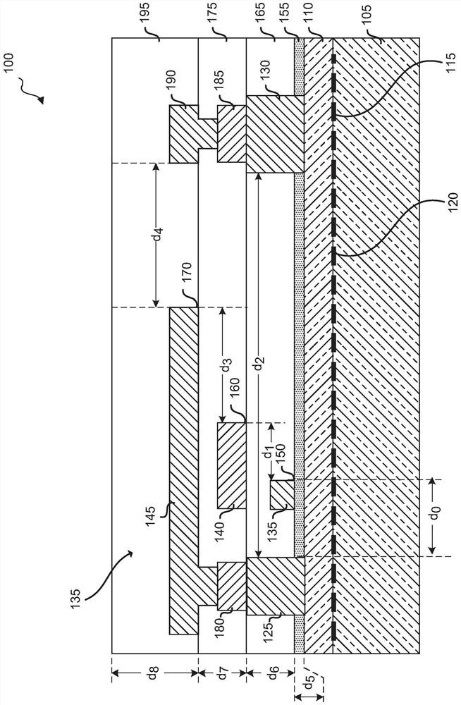
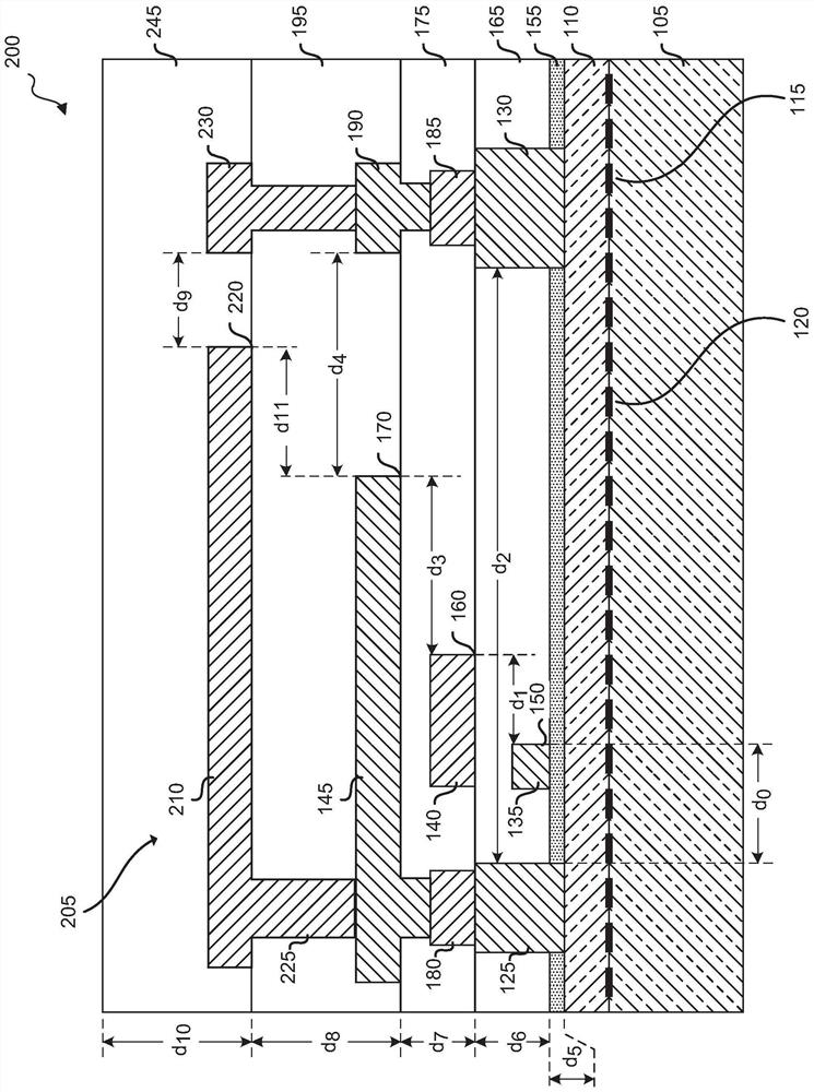
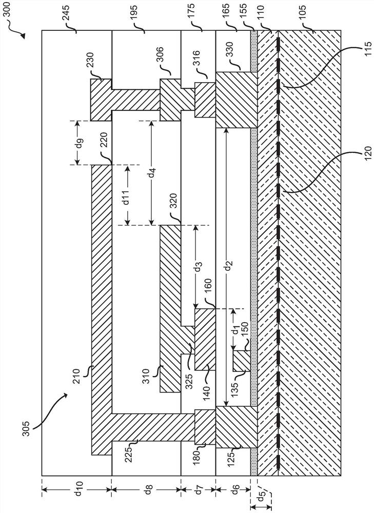
[0031] figure 1 is a schematic representation of a cross-sectional view of a lateral channel HEMT 100 . HEMT 100 includes a first semiconductor material 105 and a second semiconductor material 110 in contact with each other to form a heterojunction 115 . Due to the material properties of the semiconductor materials 105 , 110 , a two-dimensional electron gas appears 120 at the heterojunction 115 . HEMT 100 also includes source electrode 125 , drain electrode 130 and gate electrode 135 . Selective biasing of the gate electrode 135 adjusts the conductivity between the source electrode 125 and the drain electrode 130 .

[0032] HEMT 100 also includes a vertically layered field plate structure 135 . In the illustrated embodiment, the field plate structure 135 is a dual field plate structure including a gate-connected field plate 140 and a source-connected field plate 145 . The gate-connected field plate 140 is electrically connected to the gate electrode 135 . A source-connect...


PUM

PropertyMeasurementUnit
thicknessaaaaaaaaaa
thicknessaaaaaaaaaa
distanceaaaaaaaaaa

Abstract

The present invention describes a high electron mobility transistor comprising a plurality of field plates. In a first embodiment, a HEMT includes: a first semiconductor material and a second semiconductor material arranged to form a heterojunction at which a a two-dimensional electron gas; and a source electrode, a drain electrode, and a gate electrode. The gate electrode is provided to adjust conductivity in the heterojunction between the source electrode and the drain electrode. The gate has a drain side edge. A gate-connected field plate is disposed over the drain-side edge of the gate electrode and extends laterally towards the drain. A second field plate is disposed over the drain-side edge of the gate-connected field plate and extends laterally towards the drain.

Description

[0001] Cross References to Related Applications [0002] This application claims priority under 35 U.S.C. §119 to U.S. Provisional Application Serial No. 61 / 921,140, ​​filed December 27, 2013, which is incorporated herein by reference in its entirety. technical field [0003] This invention relates to high electron mobility transistors, and more particularly, to the design of field plates and other components of high electron mobility transistors. Background technique [0004] A high electron mobility transistor (HEMT)—also known as a heterojunction field effect transistor (HFET)—is a field effect transistor that includes a heterojunction that acts as the transistor channel. In HEMTs, the conductivity of the "two-dimensional electron gas" in the heterojunction channel is regulated by the gate. [0005] Although HEMTs were invented in the late 1970s and have achieved commercial success in some applications (e.g., mmWave switching), some HEMTs (e.g., Gallium Nitride-based HEM...

Claims


Application Information

Patent Timeline
Patent Type & Authority Patents(China)
IPC IPC(8): H01L29/778H01L29/40
CPCH01L29/404H01L29/7787H01L29/7786H01L29/2003H01L29/66462H01L29/518H01L29/205
Inventor A·库迪姆J·拉姆德尼L·刘
Owner POWER INTEGRATIONS INC
Features
  • Generate Ideas
  • Intellectual Property
  • Life Sciences
  • Materials
  • Tech Scout
  • Unparalleled Data Quality
  • Higher Quality Content
  • 60% Fewer Hallucinations
Learn More