Organic solar cells including group IV nanocrystals and method of manufacture

a solar cell and nanocrystal technology, applied in the field of solar cells, can solve the problems of low fill factor and short circuit current, low efficiency of known bulk heterojunction organic solar cell devices, and inefficient collection of generated excitons before they recombine, so as to increase the absorption capacity of bulk heterojunction materials

Inactive Publication Date: 2005-03-24
EVERGREEN SOLAR
View PDF5 Cites 103 Cited by
  • Summary
  • Abstract
  • Description
  • Claims
  • Application Information

AI Technical Summary

Benefits of technology

[0009] In general, in one aspect, the present invention features an improved bulk heterojunction material for use within an organic solar cell. The bulk heterojunction material includes an organic absorber and a plurality of group IV nanocrystals disposed within the organic absorber. The organic absorber (e.g., polymer) absorbs sunlight having wavelengths between about 350 nm to about 650 nm and in response generates an exciton (i.e., a boound electron / hole pair). The group IV nanocrystals (e.g., silicon nanocrystals, germanium nanocrystals, silicon-germanium nanocrystals) act not only as acceptor molecules, but also provide the bulk heterojunction material with another source of absorption. The group IV nanocrystals absorb long wavelength sunlight (e.g. about 650 nm to 1000 nm), thereby increasing the absorption capability of the bulk heterojunction material.
[0015] In general, the bulk heterojunction material including both the organic absorber and the plurality of group IV nanocrystals as described above can include one or more of the following advantages. The bulk heterojunction material of the invention can absorb a broader spectrum of light in comparison to known organic bulk heterojunction materials, such as a combination of organic polymer and fullerenes. In particular, the group IV nanocrystals can act as both an absorber and an acceptor material. As a result, more light, including light having a longer wavelength (e.g., 650 nm to 1000 nm) can be absorbed by the bulk heterojunction material and thus greater solar cell efficiency can be achieved. Moreover, because the bulk heterojunction material is formed of a higher concentration of materials that can absorb light (i.e. both the organic absorber and the nanocrystals can absorb light in comparison to just the organic absorber in known organic heterojunction materials) more excitons can be generated. As a result, better collection at the electrodes and thus better solar cell efficiencies are possible. The bulk heterojunction material of the present invention is easy to manufacture and can be produced in high yield volumes. As a result, manufacturing expenses are reduced, which leads to a reduction in solar cell costs. In addition, the bulk heterojunction material is highly flexible and durable in comparison to single crystalline homojunction materials (e.g., doped silicon wafers). As a result, solar cells manufactured with the bulk heterojunction material of the present invention are less susceptible to damage and can be used in more demanding environments.

Problems solved by technology

However the efficiency of known bulk heterojunction organic solar cell devices is less than 4%.
Some of the challenges with making efficient bulk heterojunction organic solar cells include the ability to form low resistance, low recombination contacts (the final contact will be an inorganic metal of some sort); the ability to efficiently absorb the full solar spectrum (many organic polymers absorbers cover only a portion of the solar spectrum); recombination of the holes and electrons that limit the thickness of the absorbing layer; and generally inefficient collection of the generated excitons before they recombine due to dimensions exceeding the 10 to 20 nm diffusion length of the excitons (the diffusion length of an exciton in a polymer is about 10 to 20 nm; this dimension establishes the scale needed in the microstructure of the solar cell to minimize recombination).
These limitations mean that fill factors and short circuit currents are low for organic solar cells.
However, the issues of efficiency and light absorption from the full solar spectrum are still problematic for known organic solar cells.
The organic polymers used as the photoactive material and the donor material do not absorb a significant amount of sunlight in the long wavelength region of the solar spectrum and thus limit the solar cell's efficiency.
This further limits the amount of light that can be absorbed.

Method used


Image

  • Organic solar cells including group IV nanocrystals and method of manufacture
  • Organic solar cells including group IV nanocrystals and method of manufacture
  • Organic solar cells including group IV nanocrystals and method of manufacture

Examples


Embodiment Construction

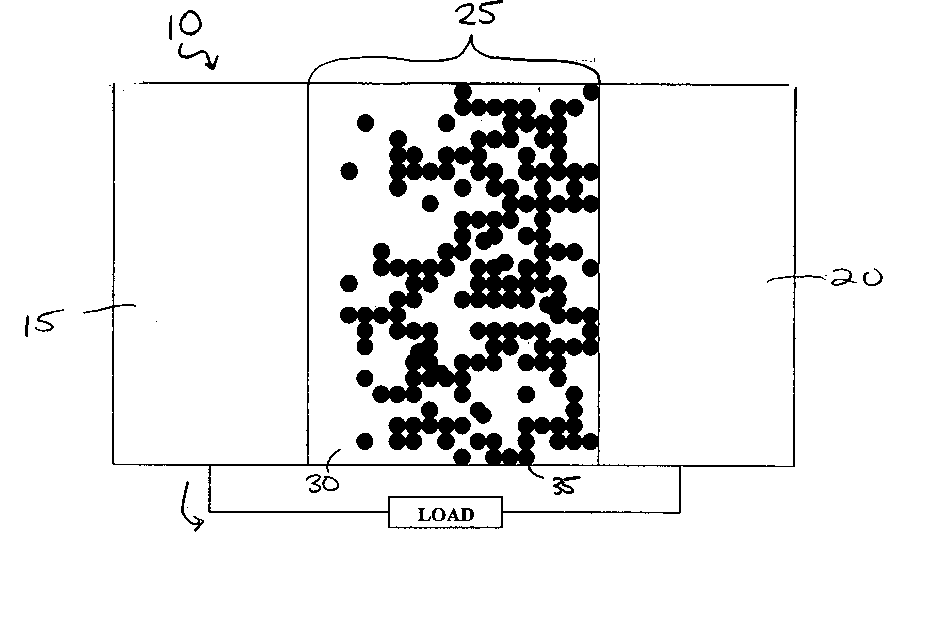
[0026] The present invention provides an improved bulk heterojunction material for an organic solar cell and a method of making the bulk heterojunction material. In general, the bulk heterojunction material includes an organic absorber (e.g., an organic polymer) and a plurality of group IV nanocrystals (e.g., silicon nanocrystals, germanium nanocrystals, silicon-germanium nanocrystals) disposed within the organic absorber.

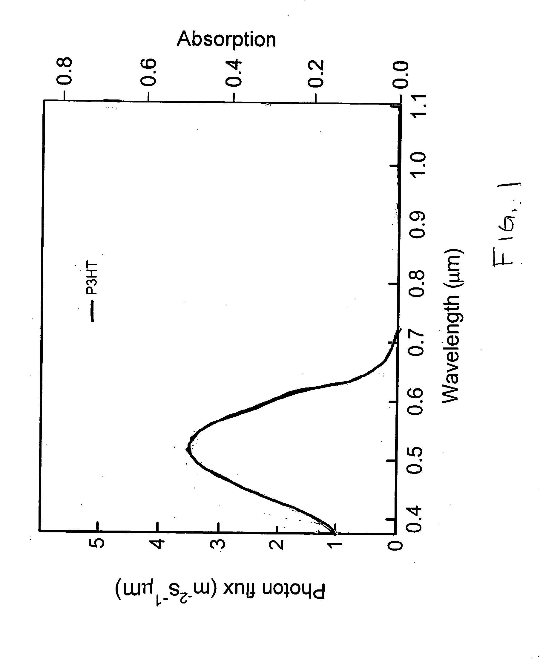
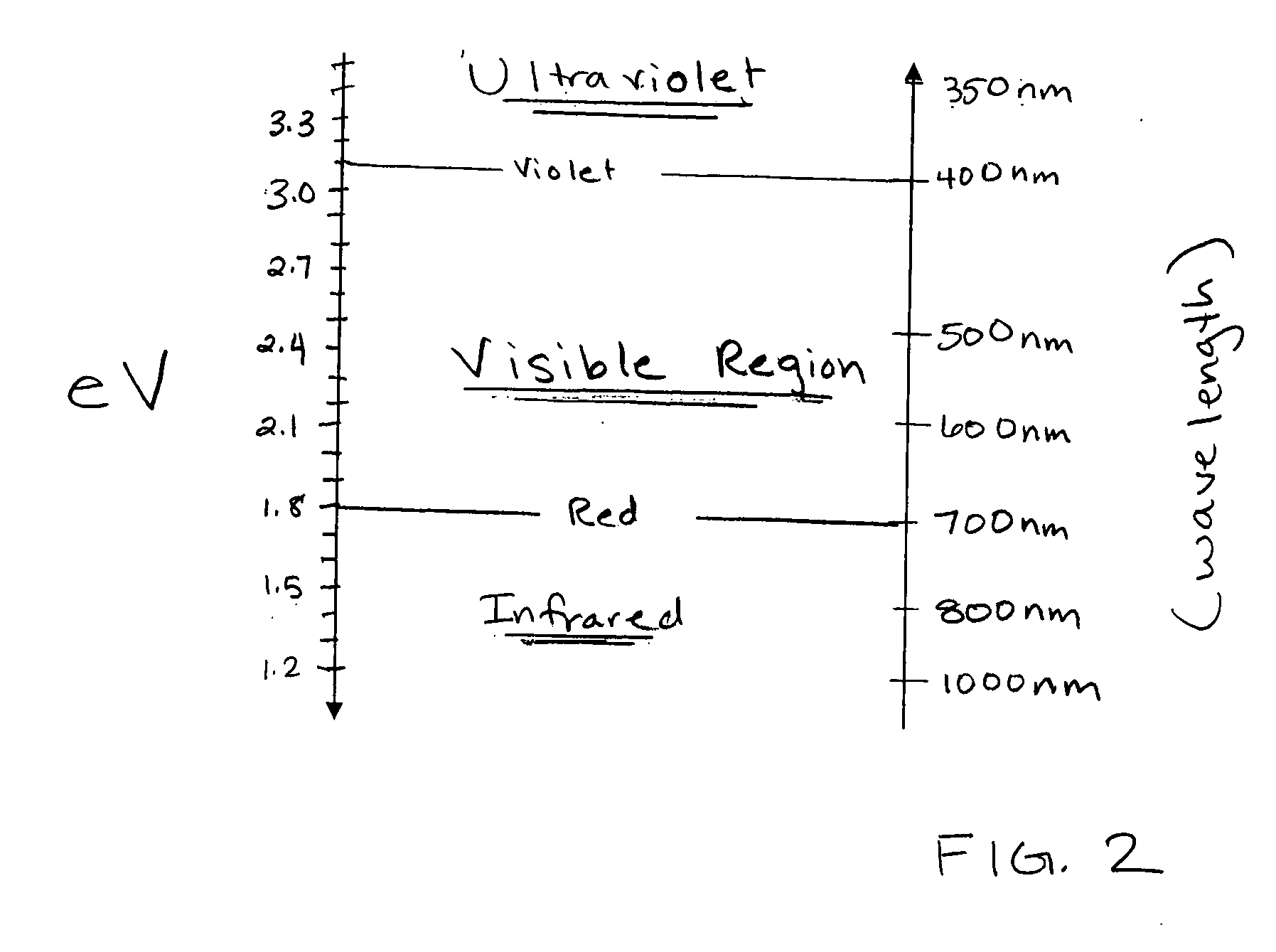
[0027] The organic absorber is a photoactive material that generates excitons (i.e., an electron / hole pair) in response to sunlight interaction. Typically, due to their band gap values (e.g., between about 1.9 eV to 3.5 eV), the organic absorber is most responsive to light having a wavelength between (350 nm and 650 nm). See FIG. 2, which shows the visible region of the electromagnetic spectrum in terms of wavelength and corresponding energies in eV. As a result, the organic absorber tends to generate excitons in response to sunlight having a wavelength between ab...


PUM

PropertyMeasurementUnit
weight percentaaaaaaaaaa

Abstract

An improved organic solar cell converts light into electricity. The organic solar cell includes a cathode, an anode, and a bulk heterojunction material disposed therebetween. The bulk heterojunction material includes a plurality of group IV nanocrystals (e.g., silicon nanocrystals) disposed within an organic absorber (e.g., an organic polymer).

Description

RELATED APPLICATIONS [0001] This application claims the benefit of the filing date of U.S. Provisional Patent Application Ser. No. 60 / 505,200, filed on Sep. 23, 2003, entitled “A Method for Forming Organic Solar Cells using Nanocrystalline Silicon” by Ginley et al., the entirety of which is incorporated herein by reference.FIELD OF THE INVENTION [0002] The invention generally relates to solar cells, and more particularly to organic solar cells, which include a mixture of an organic absorber and a plurality of group IV nanocrystals to form the bulk heterojunction material within the solar cell. BACKGROUND OF THE INVENTION [0003] Organic solar cells (also called plastic, polymer, or excitonic solar cells) have recently attracted significant interest and represent an attractive possibility for making flexible solar electric panels that offer the potential for low cost solar electricity. In general, known organic solar cells include an organic material positioned between two electrodes....

Claims


Application Information

Patent Timeline
Patent Type & Authority Applications(United States)
IPC IPC(8): H01L31/00H01L31/0384H01L51/00H01L51/30H01L51/42
CPCB82Y30/00H01L31/0384H01L51/0036Y02E10/549H01L51/4213H01L51/426H01L51/0038Y02P70/50H10K85/114H10K85/113H10K30/10H10K30/35
Inventor GINLEY, DAVID S.HANOKA, JACK I.
Owner EVERGREEN SOLAR
Why Eureka
Try Eureka