

GaN-based high electron mobility transistor
a high electron mobility, transistor technology, applied in the direction of basic electric elements, electrical apparatus, semiconductor devices, etc., can solve the problems of dangling nitrogen atom dangle bonds, large number of lattice defects in undoped gan layers, and difficulty in high speed operation of gan-based hemt, etc., to achieve the effect of high electron mobility
- Summary
- Abstract
- Description
- Claims
- Application Information
AI Technical Summary
Benefits of technology
Problems solved by technology
Method used
Image

Examples
Embodiment Construction
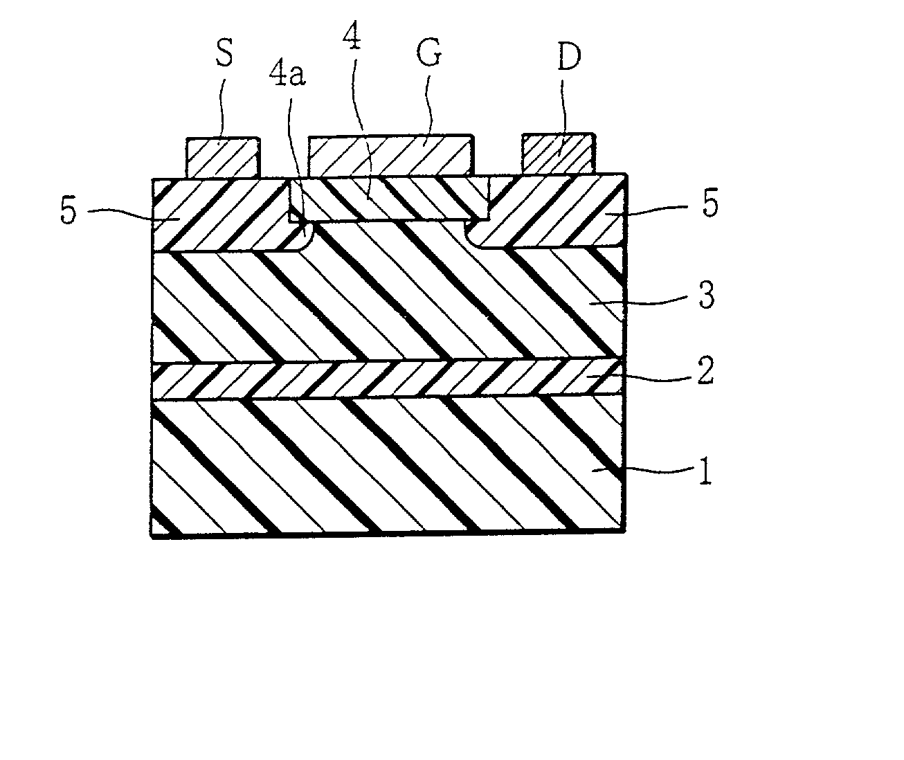
[0041] By using an ultravacuum apparatus with a growth chamber and a patterning chamber, a gas source MBE was performed to form a GaN buffer layer 2 with a thickness of 50 nm on an Si single crystal substrate 1 at a growth temperature of 640.degree. C. Metal Ga (5.times.10.sup.-7 Torr) was used as a Ga source and dimethylhydrazine (5.times.10.sup.-5 Torr) as an N source.
[0042] Then, the N source was switched to ammonia (5.times.10.sup.-5 Torr), and a gas source MBE was performed at a growth temperature of 780.degree. C., thereby forming an undoped GaN layer 3 with a thickness of 2000 nm. The carrier concentration of the undoped GaN layer 3 was controlled to 1.times.10.sup.15 cm.sup.-3 by doping a p-type impurity of Mg (1.times.10.sup.-8Torr).
[0043] In a separate experiment, the same undoped GaN layer was formed under the same conditions. When its electric resistivity was measured by a contactless-type contact resistance measurement apparatus, the reading was 100 M.OMEGA. / cm.sup.2.
[0...
PUM
 Abstract
Description
Claims
Application Information