Integration of strained Ge into advanced CMOS technology

a technology of strained ge and advanced cmos, applied in the field of pmos device hosted in strained ge, can solve the problems of high device mobility, inconvenient integration, and high difficulty in keeping carrier mobility high, and achieve the effect of high mobility and readily scalabl

Inactive Publication Date: 2005-12-29
GLOBALFOUNDRIES INC
View PDF13 Cites 353 Cited by
  • Summary
  • Abstract
  • Description
  • Claims
  • Application Information

AI Technical Summary

Benefits of technology

[0007] This invention describes an integration scheme for advanced CMOS technology which incorporates a high mobility strained Ge buried channel structure, leading to PMOS device improvement. The scheme is readily scalable with decreasing dimensions.

Problems solved by technology

As MOSFET (Metal Oxide Semiconductor Field-Effect-Transistor, a name with historic connotations meaning in general an insulated gate Field-Effect-Transistor) devices are being scaled down, the technology becomes more complex and new methods are needed to maintain the expected performance enhancement from one generation of devices to the next.
There is great difficulty in keeping carrier mobility high in devices of deeply submicron generations.
Such features are not or suitable for integration into advanced high performance CMOS technologies.

Method used


Image

  • Integration of strained Ge into advanced CMOS technology
  • Integration of strained Ge into advanced CMOS technology
  • Integration of strained Ge into advanced CMOS technology

Examples


Embodiment Construction

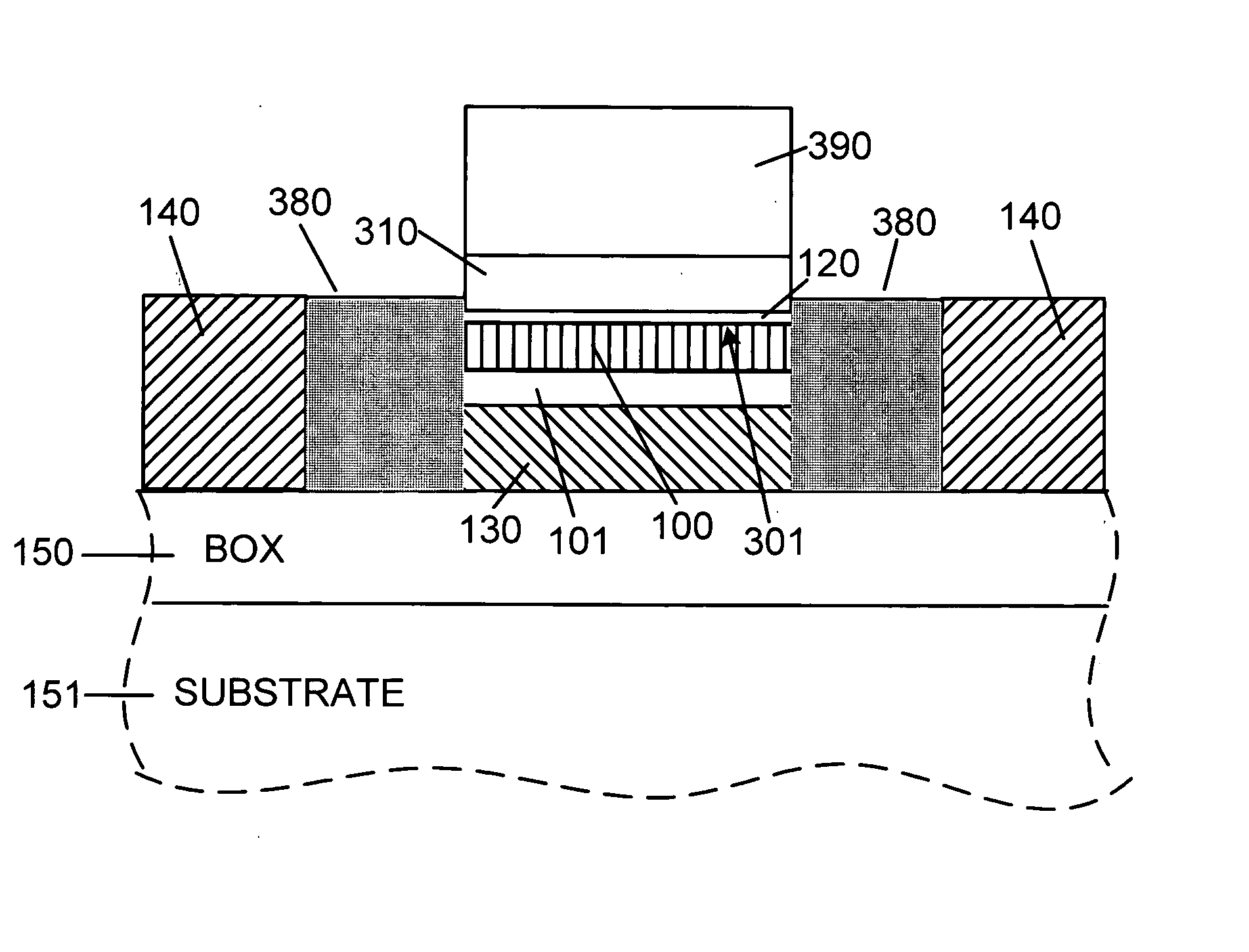
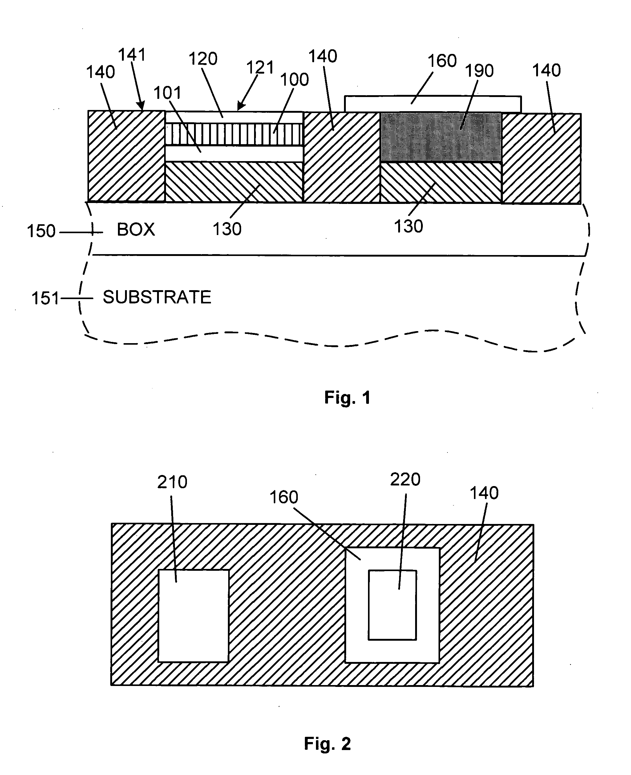
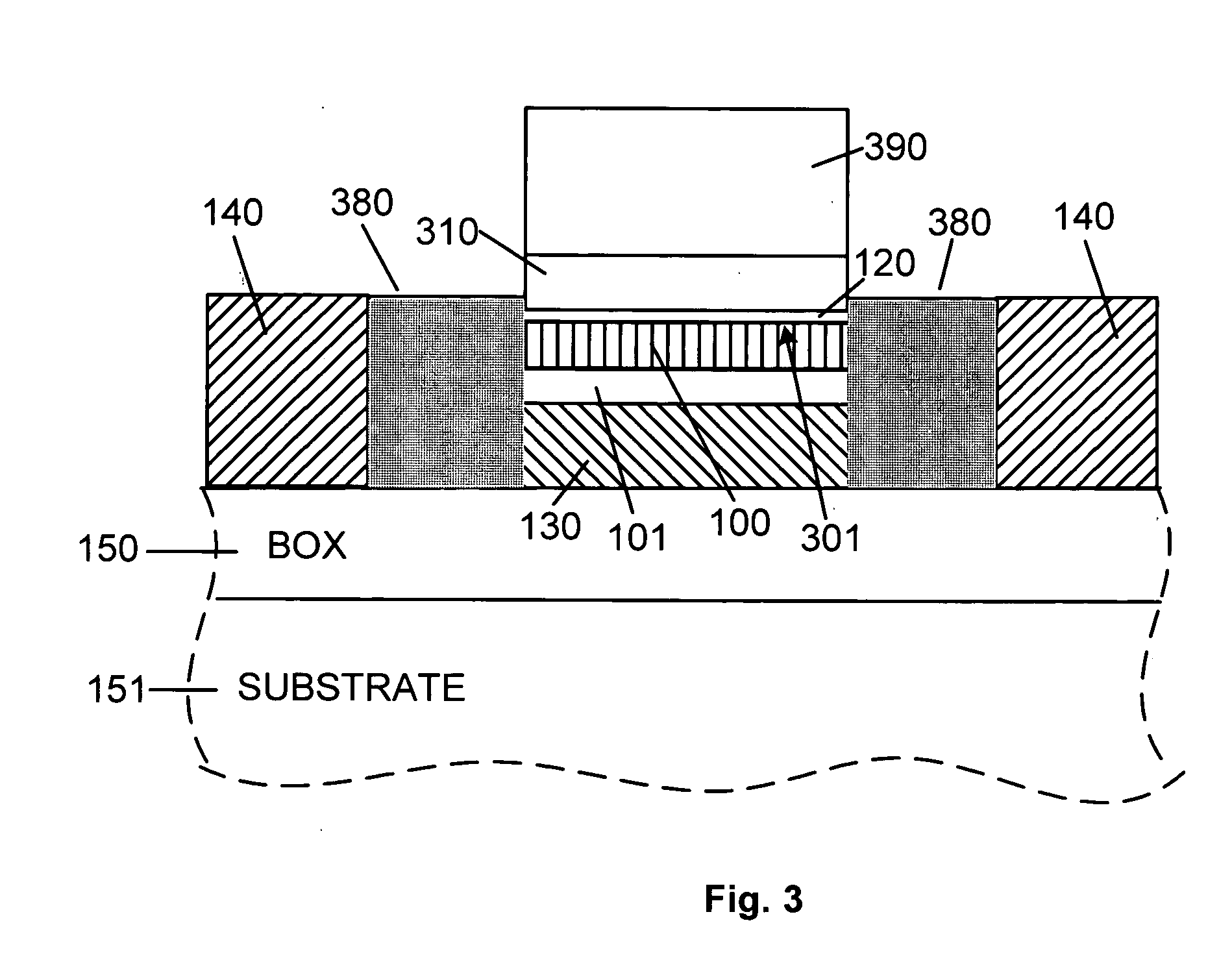
[0018] In the integration of strained Ge into advanced CMOS technology it is preferable to maintain the overall standard fabrication process of mainline Si CMOS as much as feasible. This invention integrates compressively strained Ge into such a process with changing / adding only a few steps out of the well over a hundred steps of typical advanced Si CMOS processing. In an exemplary embodiment the overall process flow of CMOS fabrication, including the strained Ge hosted PMOS, would follow these steps: Start with a silicon-on-insulator (SOI) or silicon-germanium-on-insulator (SGOI) wafer; go through the standard shallow trench isolation (STI) process, as known to one skilled in the art; cap NMOS region with a mask; open up Si or SiGe islands only in PMOS region; grow selectively Ge on top of exposed Si or SiGe surface; strip masking cap on NFET region; continue with the standard CMOS fabrication as known to one skilled in the art. This invention also teaches steps and structures whic...


PUM


Abstract

A structure and method of fabrication for PFET devices in a compressively strained Ge layer is disclosed. The fabrication method of such devices is compatible with standard CMOS technology and it is fully scalable. The processing includes selective epitaxial depositions of an over 50% Ge content buffer layer, a pure Ge layer, and a SiGe top layer. Fabricated buried channel PMOS devices hosted in the compressively strained Ge layer show superior device characteristics relative to similar Si devices.

Description

FIELD OF THE INVENTION [0001] The present invention relates to semiconductor technology and, more specifically, to a PMOS device hosted in strained Ge. This device is fabricated in a manner that it can be effectively scaled and integrated into high performance silicon based CMOS technologies. BACKGROUND OF THE INVENTION [0002] Today's integrated circuits include a vast number of devices. Smaller devices are key to enhance performance and to improve reliability. As MOSFET (Metal Oxide Semiconductor Field-Effect-Transistor, a name with historic connotations meaning in general an insulated gate Field-Effect-Transistor) devices are being scaled down, the technology becomes more complex and new methods are needed to maintain the expected performance enhancement from one generation of devices to the next. [0003] One of the most important indicators of potential device performance is the carrier mobility. There is great difficulty in keeping carrier mobility high in devices of deeply submi...

Claims


Application Information

Patent Timeline
Patent Type & Authority Applications(United States)
IPC IPC(8): H01L21/8238H01L21/84H01L27/12H01L29/06H01L29/10
CPCH01L21/823807H01L21/84H01L29/7841H01L29/1054H01L27/1203
Inventor SHANG, HUILINGIEONG, MEIKEICHU, JACK OONGUARINI, KATHRYN W.
Owner GLOBALFOUNDRIES INC
Why Eureka
Try Eureka