

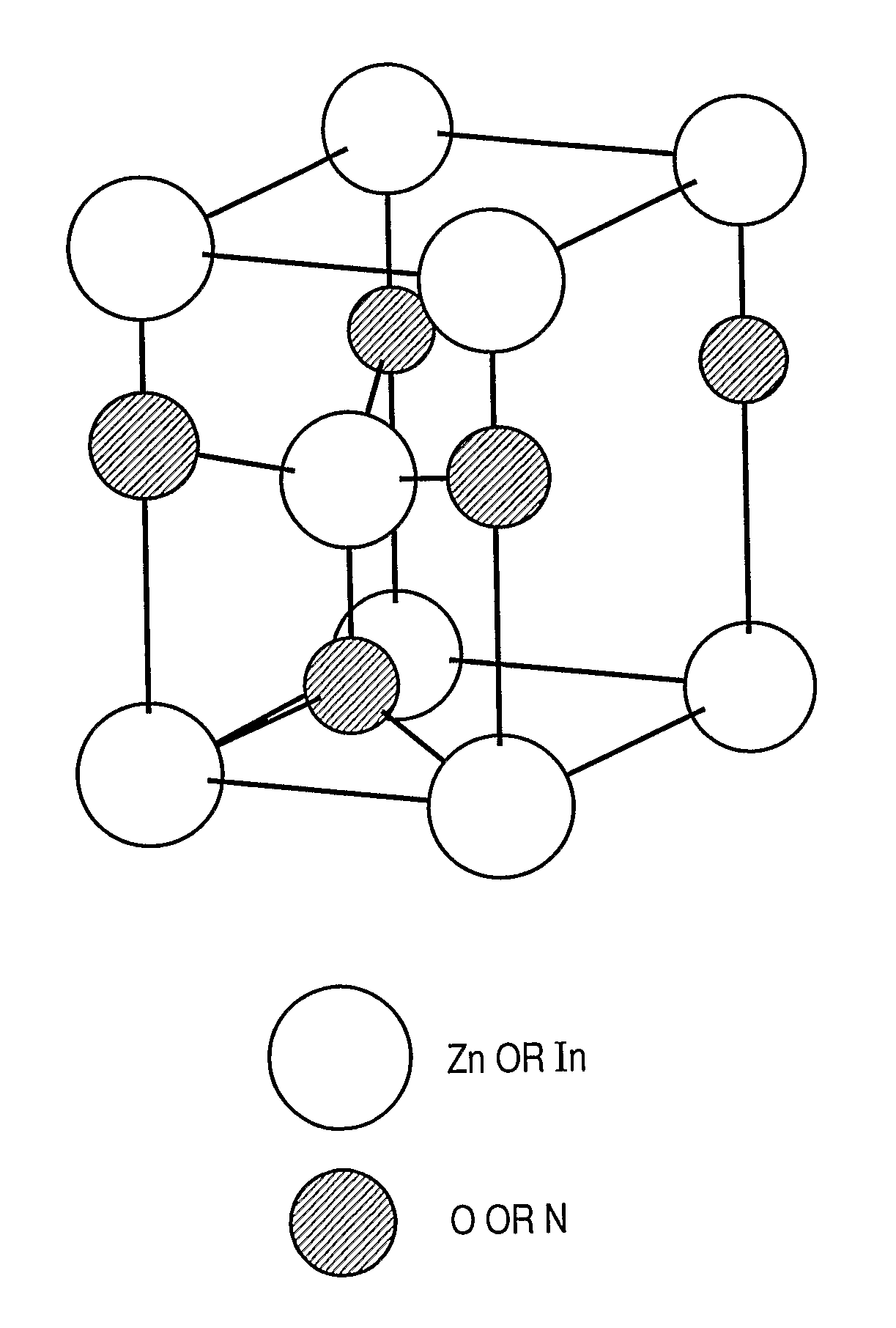
Metal oxynitride semiconductor containing zinc
a technology of metal oxynitride and semiconductor, which is applied in the direction of semiconductor devices, basic electric elements, electrical equipment, etc., can solve the problems of insufficient stability of laser beams, inability to use low-cost substrates such as resin substrates, substrates or plastic substrates, etc., and achieves high mobility and environmental stability.
- Summary
- Abstract
- Description
- Claims
- Application Information
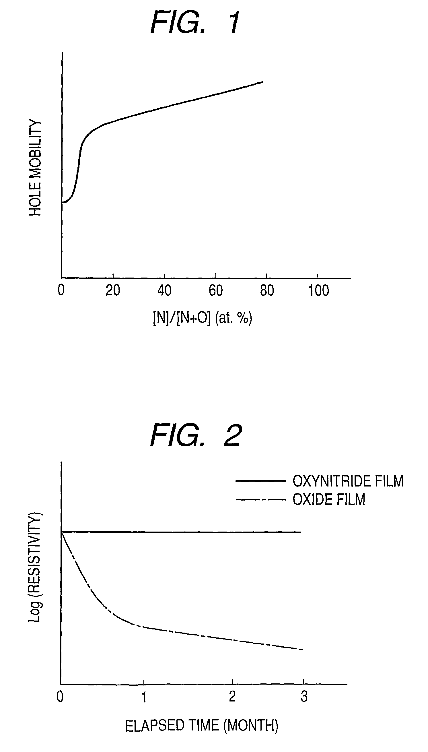
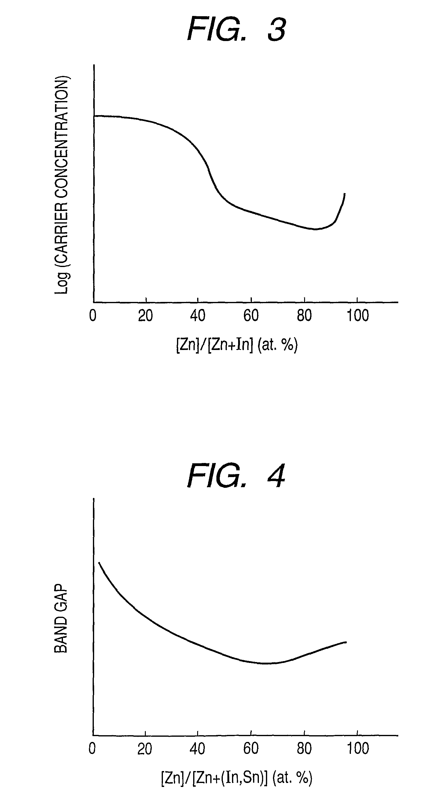
AI Technical Summary
Benefits of technology
Problems solved by technology
Method used
Image

Examples
example 1
Zn—In—ON Film, N / (N+O)=35 Atomic Percent
[0088]In this example, a Zn—In—ON film was formed on a glass and silicon substrates in an atmosphere containing a mixture of argon and nitrogen by RF sputtering using a radical source.
[0089]A 2-inch sintered material having a composition of ZnO and a 2-inch sintered material having a composition of In2O3 (each of which has a purity of 99.9%) were used as targets (material sources). Input RF powers are 50 W (ZnO) and 30 W (In2O3). The radical source is excited by electron cyclotron resonance plasma. Input microwave power is 80 W. In this example, N radicals generated from the radical source are introduced into the sputtering film formation atmosphere to control the nitrogen concentration in the film. The distance between each of the targets and the substrate was set to approximately 10 cm. The substrate temperature during film formation was set to 25° C. The Zn—In—ON film was formed in the atmosphere containing the mixture of argon and nitrogen...
example 2
Zn—In—ON Film, N / (N+O)=42 Atomic Percent, Zn / (Zn+In =85 Atomic Percent
[0104]In this example, a Zn—In—ON film was formed on a glass substrate in an atmosphere containing a mixture of argon and nitrogen by RF sputtering using a radical source.
[0105]A 2-inch sintered material having a composition of ZnO and a 2-inch sintered material having a composition of In2O3 (each of which has a purity of 99.9%) were used as targets (material sources). Input RF powers are 65 W (ZnO) and 12 W (In2O3). The radical source is excited by electron cyclotron resonance plasma. Input microwave power is 150 W. In this example, N radicals generated from the radical source are introduced into the sputtering film formation atmosphere to control nitrogen concentration in the film. The distance between each of the targets and the substrate was set to approximately 10 cm. The substrate temperature during film formation was set to 25° C. The Zn—In—ON film was formed in the atmosphere containing the mixture of argo...
example 3
Transistor using Zn—In—ON for Active Layer
[0111]In this example, the top-gate Zn—In—ON thin film transistor as illustrated in FIG. 5 was manufactured.
[0112]A Zn—In—ON oxynitride film used as the active layer 12 was deposited on the glass substrate 11 in an atmosphere containing a mixture of argon and nitrogen by RF sputtering using a radical source. A 2-inch sintered material having a composition of ZnO and a 2-inch sintered material having a composition of In2O3 (each of which has a purity of 99.9%) were used as targets (material sources). Input RF powers are 50 W (ZnO) and 30 W (In2O3). The radical source is excited by electron cyclotron resonance plasma. Input microwave power is 80 W. In this example, N radicals generated from the radical source are introduced into the sputtering film formation atmosphere to control the nitrogen concentration in the film. The distance between each of the targets and the substrate was set to approximately 10 cm. The substrate temperature during fi...
PUM
| Property | Measurement | Unit |
|---|---|---|
| band gap | aaaaa | aaaaa |
| humidity | aaaaa | aaaaa |
| temperature | aaaaa | aaaaa |
Abstract
Description
Claims
Application Information