A dual-channel ATA protocol bridging device based on nand FLASH interface

A technology of ATA protocol and bridging device, which is applied in the field of microelectronics to achieve the effect of broad application prospects, strong flexibility, and guaranteed correctness

Active Publication Date: 2018-08-07
SHANDONG SINOCHIP SEMICON
View PDF7 Cites 0 Cited by
  • Summary
  • Abstract
  • Description
  • Claims
  • Application Information

AI Technical Summary

Problems solved by technology

[0006] At present, there is no device that converts ONFI to PATA, ONFI to SATA, TOGGLE to PATA, and TOGGLE to SATA.

Method used


Image

  • A dual-channel ATA protocol bridging device based on nand FLASH interface
  • A dual-channel ATA protocol bridging device based on nand FLASH interface
  • A dual-channel ATA protocol bridging device based on nand FLASH interface

Examples


Embodiment Construction

[0043] In order to facilitate those skilled in the art to better understand the present invention, the present invention will be described in further detail below in conjunction with the accompanying drawings and specific embodiments. The following is only exemplary and does not limit the protection scope of the present invention.

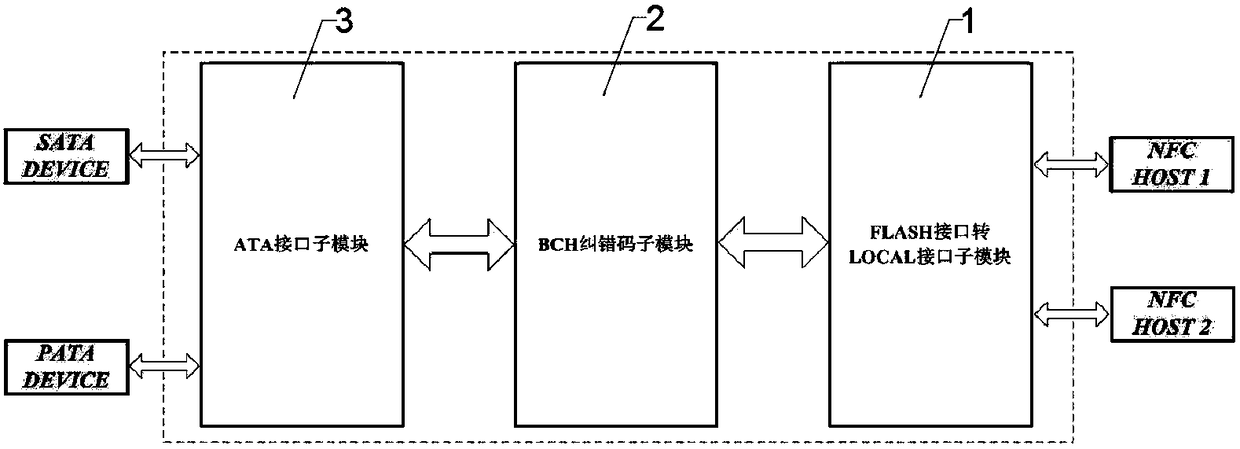
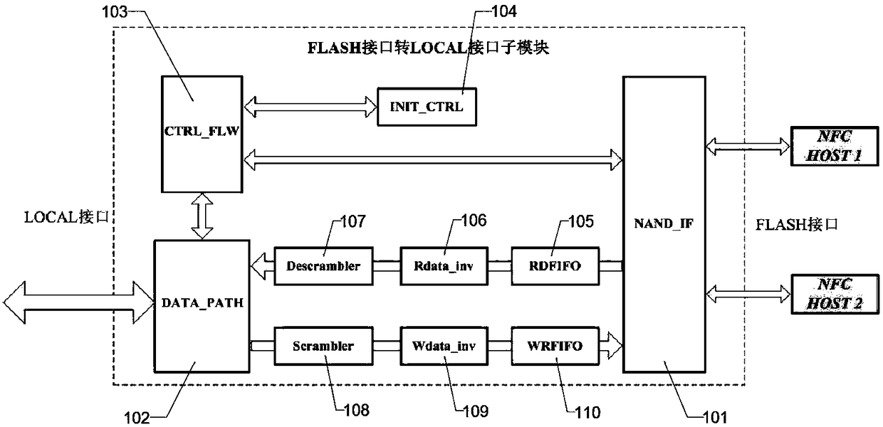
[0044] The present invention is based on the dual-channel ATA protocol bridging device of NAND FLASH interface, as figure 1 As shown, it includes: FLASH interface to LOCAL interface sub-module 1, BCH error correction code sub-module 2 and ATA interface sub-module 3. The FLASH interface to LOCAL interface submodule 1 is responsible for controlling the reading and writing of data with the external FLASH host controller, and simultaneously converts it to a LOCAL bus for transmission. The FLASH interface to LOCAL interface submodule 1 converts the command received from the host controller Perform operations such as reading, analysis, execution, and fee...


PUM


Abstract

The present invention is based on the dual-channel ATA protocol bridging device of the NAND FLASH interface, including the FLASH interface to the LOCAL interface submodule, the BCH error correction code submodule and the ATA interface submodule, between the FLASH interface to the LOCAL interface submodule and the external FLASH host controller, There are two-way communication connections between the FLASH interface to LOCAL interface submodule and the BCH error correction code submodule, between the BCH error correction code submodule and the ATA interface submodule, and between the ATA interface submodule and the external hard disk. The user only needs to design a simple driver program to configure the relevant parameters in the device, and then use the existing low-cost storage device to apply it to the new storage system, and complete the four functions of converting ONFI to PATA, ONFI to SATA, TOGGLE to PATA, and TOGGLE to SATA. Various application functions, strong flexibility and broad application prospects.

Description

technical field [0001] The invention relates to a dual-channel ATA protocol bridging device based on a NAND FLASH interface, which belongs to the technical field of microelectronics. Background technique [0002] NAND FLASH MEMORY has the advantages of small storage unit size, fast programming speed, and short erasing time. It has more and more applications and is a very popular storage medium in the industry. According to different manufacturers, the NAND FLASH interface standard is divided into ONFI and Toggle. Intel, Micron, and Hynix adopt the ONFI interface standard; Toshiba and Samsung adopt the Toggle standard. [0003] At present, a variety of host-side controllers based on this interface technology have appeared, such as a multi-channel NAND FLASH controller disclosed in Chinese patent CN105138470A; a multi-channel FLASH controller disclosed in Chinese patent CN204270293U; a NAND FLASH controller and its application. [0004] Because NAND FLASH adopts multi-layer ...

Claims


Application Information

Patent Timeline
Patent Type & Authority Patents(China)
IPC IPC(8): G06F13/40G06F13/42
CPCG06F13/4068G06F13/4239G06F13/4282G06F2213/0032G06F2213/3852
Inventor 刘奇浩孙晓宁刘大铕徐毅松李文军
Owner SHANDONG SINOCHIP SEMICON
Why Eureka
Try Eureka