Array substrate mother board, manufacturing method of array substrate mother board, display device and manufacturing method of display device

The technology of an array substrate and its manufacturing method, which is applied in the display field, can solve problems such as the inability to load the driving signal of the driving circuit, and achieve the effect of saving mold opening costs and realizing narrow borders

Inactive Publication Date: 2016-07-20
BOE TECH GRP CO LTD +1
View PDF2 Cites 24 Cited by
  • Summary
  • Abstract
  • Description
  • Claims
  • Application Information

AI Technical Summary

Problems solved by technology

However, the gate lines and data lines on the existing array substrate motherboards are arranged crosswise. Therefore, if the array substrate motherboard is freely cut, the gate lines and data lines may be cut off, resulting in the inability to drive the drive circuit. Signal loading on gate and data lines

Method used


Image

  • Array substrate mother board, manufacturing method of array substrate mother board, display device and manufacturing method of display device
  • Array substrate mother board, manufacturing method of array substrate mother board, display device and manufacturing method of display device
  • Array substrate mother board, manufacturing method of array substrate mother board, display device and manufacturing method of display device

Examples


Embodiment 1

[0048] This embodiment provides a method for manufacturing an array substrate motherboard, including:

[0049] providing a base substrate;

[0050] forming a plurality of via holes through the base substrate;

[0051] forming a conductive post in the via hole;

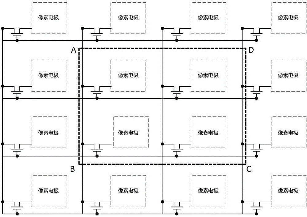
[0052] A plurality of display units arranged in an array are formed on the first surface of the base substrate, each display unit includes a thin film transistor and a pixel electrode, and the gate electrode and source electrode of each thin film transistor are respectively electrically connected to a conductive column.

[0053] In this embodiment, a plurality of via holes penetrating the base substrate are formed on the base substrate, conductive pillars are formed in the via holes, a display unit is formed on one surface of the base substrate, and the gate electrode and the gate electrode of the thin film transistor in the display unit are The source electrodes are respectively electrically connected to a conductiv...

Embodiment 2

[0060] This embodiment provides an array substrate mother board, which is manufactured by using the manufacturing method described in Embodiment 1. The array substrate includes a base substrate, and the base substrate includes a plurality of processes passing through the base substrate. A conductive column is formed in the via hole, and a plurality of display units arranged in an array are formed on the first surface of the base substrate, each display unit includes a thin film transistor and a pixel electrode, and the gate of each thin film transistor The electrode and the source electrode are respectively electrically connected to a conductive column.

[0061] In this embodiment, the base substrate includes a plurality of via holes penetrating the base substrate. Conductive pillars are formed in the via holes. A display unit is arranged on one surface of the base substrate. The gate electrode and source of the thin film transistor in the display unit The electrodes are respe...

Embodiment 3

[0068] This embodiment provides a method for manufacturing a display device, including:

[0069] cutting the above-mentioned array substrate mother board to obtain an array substrate with a preset size;

[0070] A driving circuit is adhered on the second surface of the array substrate opposite to the first surface, and a conductive lead connecting the conductive column and the driving circuit is formed.

[0071] In this embodiment, the array substrate motherboard can be freely cut. After the array substrate motherboard is cut into any shape and size, the drive circuit can be attached to the other surface of the substrate substrate, and the conductive lead and conductive The pillar realizes the connection between the driving circuit and the electrode of the thin film transistor, so that the driving signal is loaded into the display unit, and the display unit is driven to display. Through the technical solution of the present invention, it is possible to cut the motherboard of ...


PUM


Abstract

The invention provides an array substrate mother board, a manufacturing method of the array substrate mother board, a display device and a manufacturing method of the display device, and belongs to the technical field of display. The manufacturing method of the array substrate mother board includes the steps that a substrate is provided; multiple via holes penetrating through the substrate are formed; conductive columns are formed in the via holes; multiple display units arranged in an array are formed on the first surface of the substrate, each display unit comprises a thin film transistor and a pixel electrode, and a gate electrode and a source electrode of each thin film transistor are electrically connected with one conductive column. By means of the technical scheme, the array substrate mother board can be cut into any shape and size according to requirements, and display devices in various sizes are obtained.

Description

technical field [0001] The present invention relates to the field of display technology, in particular to an array substrate motherboard and a manufacturing method thereof, a display device and a manufacturing method thereof. Background technique [0002] In the prior art, the size of the array substrate is fixed. However, some users wish to be able to freely cut the array substrate mother board, that is, not to limit the size and shape of the array substrate after cutting. However, the gate lines and data lines on the existing array substrate motherboards are arranged crosswise. Therefore, if the array substrate motherboard is freely cut, the gate lines and data lines may be cut off, resulting in failure to drive the drive circuit. Signals are applied to the gate and data lines. Contents of the invention [0003] The technical problem to be solved by the present invention is to provide an array substrate motherboard and its manufacturing method, a display device and its...

Claims


Application Information

Patent Timeline
Patent Type & Authority Applications(China)
IPC IPC(8): H01L27/12G09F9/302
Inventor 杨照坤王志东邱云
Owner BOE TECH GRP CO LTD
Why Eureka
Try Eureka