A hasti filling process

A process and film layer technology, applied in the field of shallow trench filling process, can solve the problems of large heater damage, waste, particle contamination, etc., and achieve the effect of reducing the frequency of replacing heaters, ensuring capacity utilization, and uniform thickness distribution

Active Publication Date: 2019-01-22
SEMICON MFG INT (SHANGHAI) CORP
View PDF4 Cites 0 Cited by
  • Summary
  • Abstract
  • Description
  • Claims
  • Application Information

AI Technical Summary

Problems solved by technology

[0002] Using high aspect ratio shallow trench isolation (High Aspect Shallow Trench Isolation, HASTI) process on in situ steam generation wafer (ISSG wafer) and bare wafer (Bare wafer) deposition rate (deposition rate) , dep rate) there is a difference, the research found that the correlation with the hardware equipment is relatively large, it may be that the heater has been used for a long time, and there is a residual film on the edge of the heater that cannot be removed, which causes the thickness of the wafer to deviate from the range (range, the thickness of the wafer The difference between the maximum value and the minimum value) is too large, and the wafer cannot be processed normally
[0003] At present, one method is to solve the residual film on the edge of the heater by polishing the heater, but the effect is not obvious and the damage to the heater is relatively large, and it is easy to produce particle pollution. Another method is to replace the A new heater, but the heater is expensive, it is a waste to assume that the heater must be replaced once the range is abnormal, and due to the particularity of the shallow trench insulation process with a high aspect ratio, the output per hour (wafer per hour, WPH) is slow, and usually semiconductor processing equipment preventive maintenance (Preventive Maintenance, PM) will take a lot of time to fine tune the process plan (fine tune recipe), which is not conducive to the maintenance of semiconductor processing equipment by process engineers and equipment engineers , the available time of semiconductor processing equipment is greatly reduced, which has a great impact on the company's production capacity

Method used


Image

  • A hasti filling process
  • A hasti filling process
  • A hasti filling process

Examples


Embodiment Construction

[0030] The following will clearly and completely describe the technical solutions in the embodiments of the present invention with reference to the accompanying drawings in the embodiments of the present invention. Obviously, the described embodiments are only some, not all, embodiments of the present invention. Based on the embodiments of the present invention, all other embodiments obtained by persons of ordinary skill in the art without creative efforts fall within the protection scope of the present invention.

[0031] It should be noted that, in the case of no conflict, the embodiments of the present invention and the features in the embodiments can be combined with each other.

[0032] The present invention will be further described below in conjunction with the accompanying drawings and specific embodiments, but not as a limitation of the present invention.

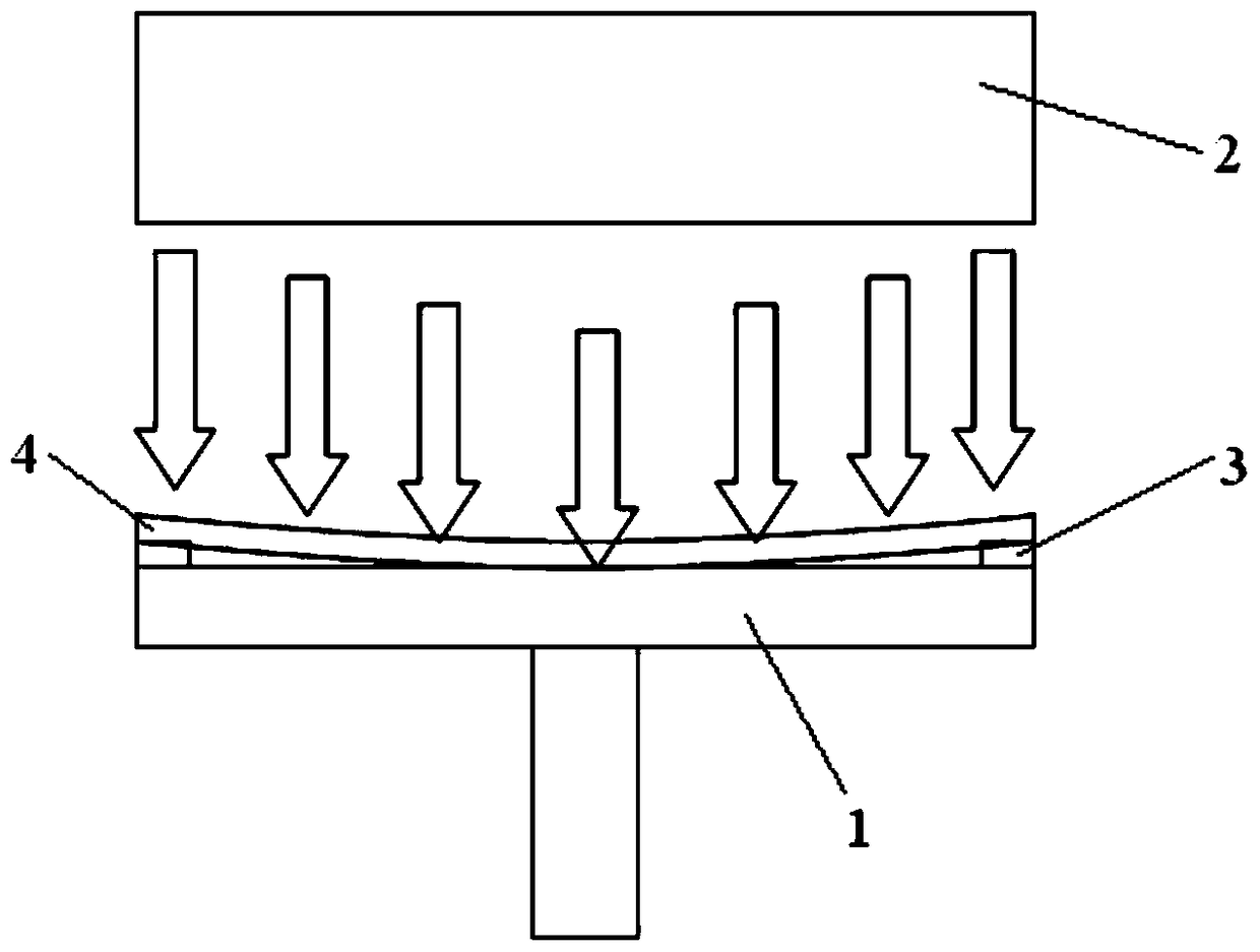
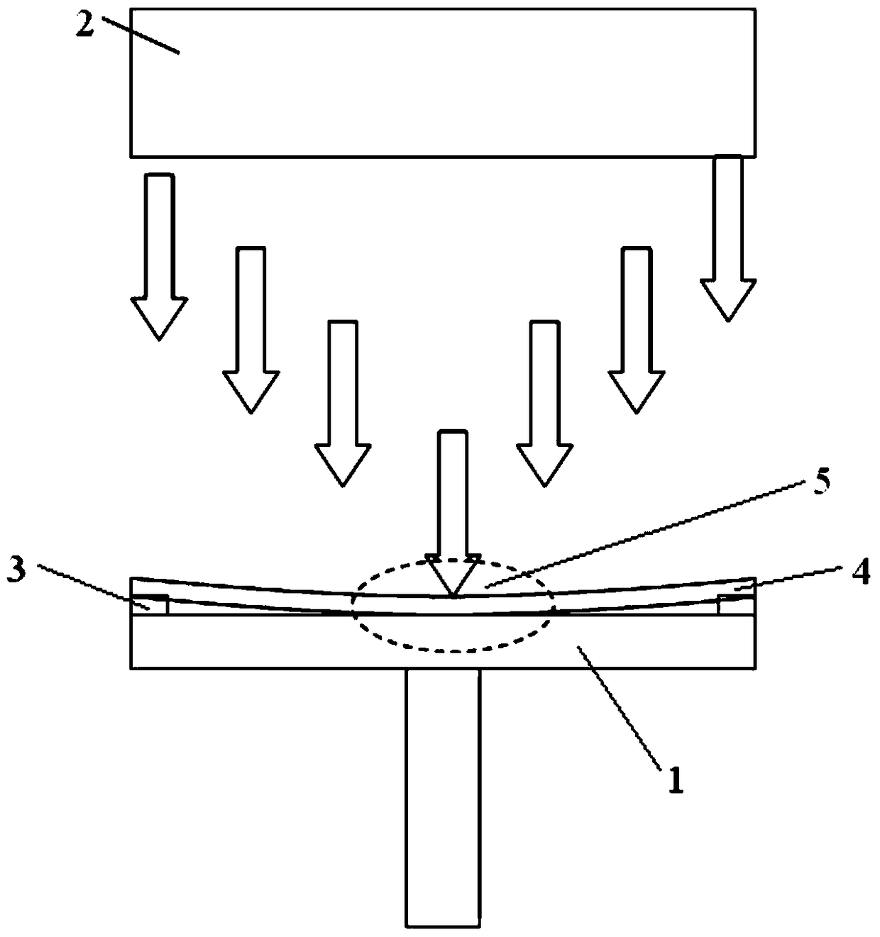
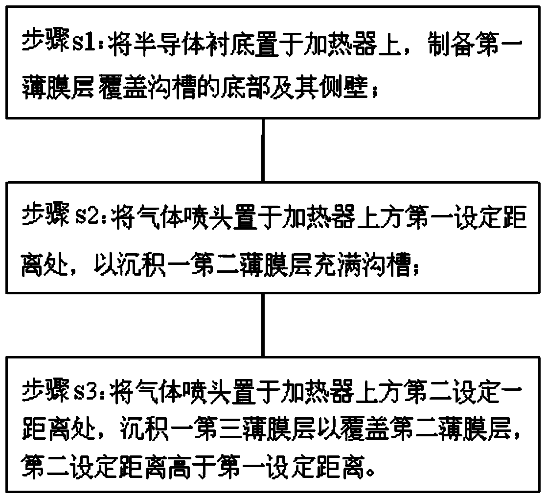
[0033] refer to figure 1 , figure 2 , image 3 , Figure 4 , a HASTI filling process, wherein, after formin...


PUM


Abstract

The invention relates to the technical field of semiconductors, and particularly relates to a shallow trench filling process. According to the HASTI (High Aspect Shallow Trench Isolation) filling process, a plurality of trenches are formed in a semiconductor substrate, and the trenches are filled through the following steps in a reaction chamber provided with a gas nozzle and a heater. The HASTI filling process specifically comprises the steps of placing the semiconductor substrate on the heater and preparing a first film layer to cover the bottom part and the side wall of each trench, placing the gas nozzle a first set distance away above the heater so as to deposit a second film layer filling the trenches, and placing the gas nozzle a second set distance away above the heater and depositing a third film layer so as to cover the second film layer, wherein the second set distance is higher than the first set distance. The HASTI filling process solves problems existing in hardware under the condition of ensuring the process safety through a process scheme of fine tuning, the thickness distribution of a wafer on which the HASTI process is implemented is more uniform, and the thickness range is improved; and the capacity utilization of a company is ensured at the same time.

Description

technical field [0001] The invention relates to the technical field of semiconductors, in particular to a shallow trench filling process. Background technique [0002] Using high aspect ratio shallow trench isolation (High Aspect Shallow Trench Isolation, HASTI) process on in situ steam generation wafer (ISSG wafer) and bare wafer (Bare wafer) deposition rate (deposition rate) , dep rate) there is a difference, the research found that the correlation with the hardware equipment is relatively large, it may be that the heater has been used for a long time, and there is a residual film on the edge of the heater that cannot be removed, which causes the thickness of the wafer to deviate from the range (range, the thickness of the wafer The difference between the maximum value and the minimum value) is too large, and the wafer cannot be processed normally. [0003] At present, one method is to solve the residual film on the edge of the heater by polishing the heater, but the effe...

Claims


Application Information

Patent Timeline
Patent Type & Authority Patents(China)
IPC IPC(8): H01L21/762
Inventor 贡禕琪陈志刚
Owner SEMICON MFG INT (SHANGHAI) CORP
Why Eureka
Try Eureka