Method for preparing mono-crystalline oxide resistive random access memory by utilizing ion injection and stripping technology

A technology of single crystal oxide and resistive memory, which is applied in the direction of electrical components, etc., can solve the problem of device parameter stability and optimization, reliability research, and the inability to grow single crystal oxide films, amorphous and polycrystalline films. Random distribution and other issues, to achieve the effect of reducing the total ion implantation dose, shortening the preparation cycle, and improving the integration and design flexibility

Active Publication Date: 2016-08-24
SHANGHAI NOVEL SI INTEGRATION TECH CO LTD
View PDF6 Cites 12 Cited by
  • Summary
  • Abstract
  • Description
  • Claims
  • Application Information

AI Technical Summary

Problems solved by technology

However, there are many problems in these traditional thin film preparation methods, for example, it is generally necessary to grow oxide thin films at relatively high temperatures, and it is difficult to be compatible with existing CMOS processes
In addition, due to factors such as lattice mismatch, thermal mismatch, and interface defects, these traditional thin film preparation methods cannot grow high-quality single crystal oxide thin films on polycrystalline metal bottom electrodes.
The resistive switching properties of materials are closely related to the defects in the material. The problems of amorphous or polycrystalline thin films as resistive switching oxide dielectric layers include: On the one hand, there are many different defects in both amorphous and polycrystalline thin films , which is a great challenge for the study of the resistance switching mechanism of materials; on the other hand, the distribution of defects in amorphous and polycrystalline thin films is random, which is very important for reducing device size, stabilizing and optimizing device parameters, reliability Research, etc. are the bottlenecks that are difficult to break through

Method used


Image

  • Method for preparing mono-crystalline oxide resistive random access memory by utilizing ion injection and stripping technology
  • Method for preparing mono-crystalline oxide resistive random access memory by utilizing ion injection and stripping technology
  • Method for preparing mono-crystalline oxide resistive random access memory by utilizing ion injection and stripping technology

Examples


Embodiment Construction

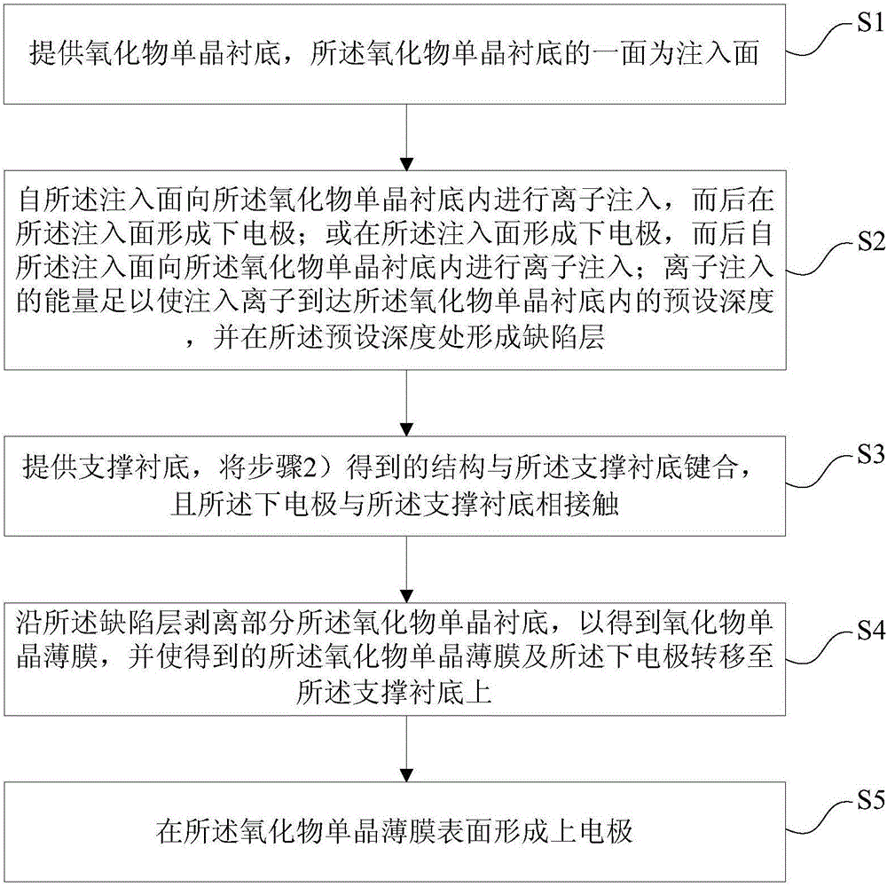
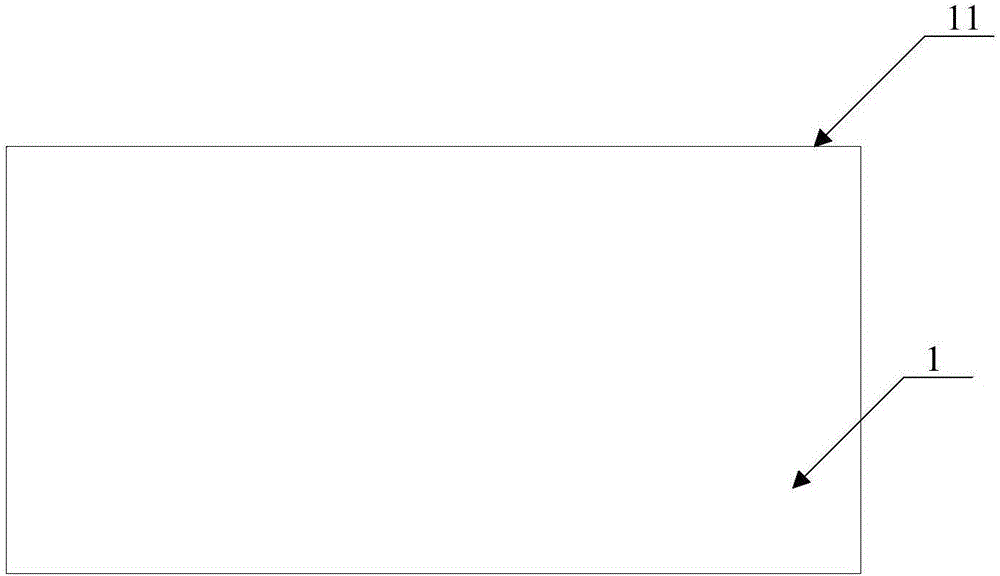
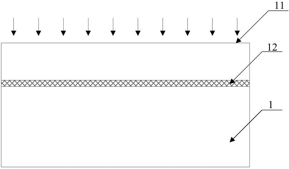
[0037] Embodiments of the present invention are described below through specific examples, and those skilled in the art can easily understand other advantages and effects of the present invention from the content disclosed in this specification. The present invention can also be implemented or applied through other different specific implementation modes, and various modifications or changes can be made to the details in this specification based on different viewpoints and applications without departing from the spirit of the present invention.

[0038] see Figure 1 to Figure 10. It should be noted that the diagrams provided in this embodiment are only schematically illustrating the basic idea of ​​the present invention, although only the components related to the present invention are shown in the diagrams rather than the number, shape and Dimensional drawing, the type, quantity and proportion of each component can be changed arbitrarily during actual implementation, and th...


PUM

PropertyMeasurementUnit
thicknessaaaaaaaaaa
thicknessaaaaaaaaaa

Abstract

The invention provides a method for preparing a mono-crystalline oxide resistive random access memory by utilizing an ion injection and stripping technology. The method comprises the following steps: (1) providing an oxide mono-crystal substrate; (2) carrying out ion injection in the oxide mono-crystal substrate from an injection surface and forming a lower electrode under the injection surface; or forming a lower electrode on the injection surface and then carrying out the ion injection in the oxide mono-crystal substrate from the injection surface; (3) providing a supporting substrate and bonding the structure obtained by the step (2) with the supporting substrate; (4) stripping one part of the oxide mono-crystal substrate along a defect layer to obtain an oxide mono-crystalline thin film and transferring the obtained oxide mono-crystalline thin film and lower electrode onto the supporting substrate; (5) forming an upper electrode on the surface of the oxide mono-crystalline thin film. With the adoption of the method provided by the invention, a total ion injection dosage needed for stripping and transferring the thin film is effectively reduced, so that a preparation period is shortened and the production cost is saved; meanwhile, the method can also be used for solving the problem that part of materials are injected through single ions and stripping cannot be realized.

Description

technical field [0001] The invention belongs to the technical field of semiconductor preparation, and in particular relates to a method for preparing a single crystal oxide resistive variable memory by using ion implantation stripping technology. Background technique [0002] Non-volatile memory is an important part of the semiconductor field, and occupies a pivotal position in the semiconductor industry. With the advancement of technology in recent years and the continuous popularization of consumer electronic products such as smartphones, mobile storage, and tablet computers, the consumption of non-volatile memory has been greatly promoted. The global memory market has a strong demand for non-volatile memory Demand has increased dramatically. Not only that, the market's requirements for memory are also increasing, such as high capacity, high speed, low power consumption, low price and so on. These requirements have further promoted the continuous development of existing ...

Claims


Application Information

Patent Timeline
Patent Type & Authority Applications(China)
IPC IPC(8): H01L45/00
CPCH10N70/043H10N70/011
Inventor 欧欣游天桂黄凯贾棋伊艾伦王曦
Owner SHANGHAI NOVEL SI INTEGRATION TECH CO LTD
Why Eureka
Try Eureka