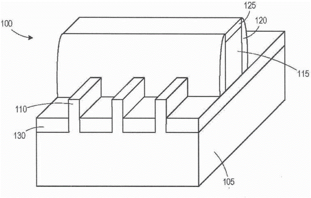
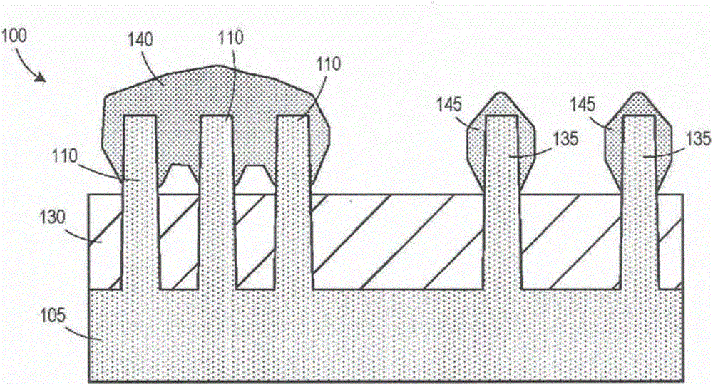
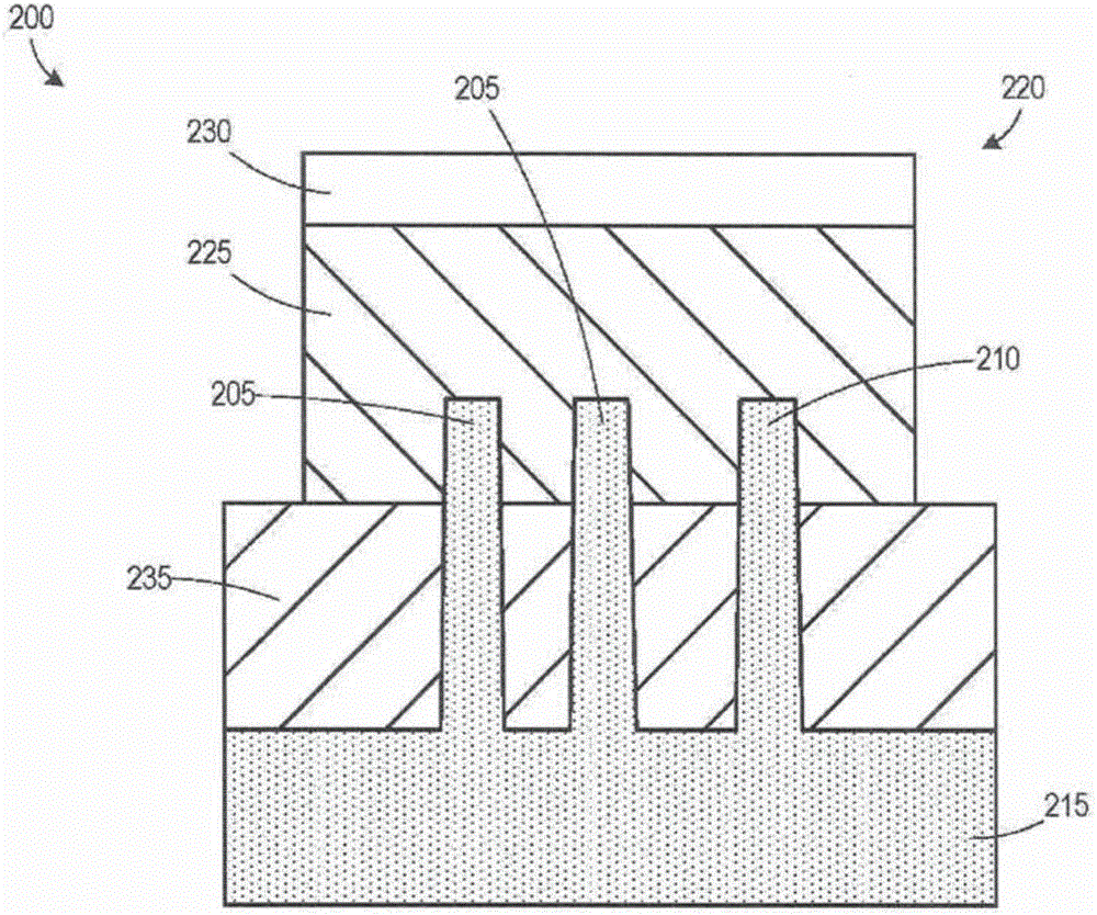
Cap layer for spacer-constrained epitaxially grown material on fins of a finfet device
A technology of epitaxial material and capping layer, applied in electrical components, semiconductor devices, electric solid devices, etc., can solve problems such as damage function and resistance difference
- Summary
- Abstract
- Description
- Claims
- Application Information
AI Technical Summary
Problems solved by technology
Method used
Image

Examples
Embodiment Construction
[0050] Various exemplary embodiments of the invention are described below. In the interest of clarity, all features of an actual implementation will be described in this specification. It should be understood, of course, that in developing any such practical embodiment, a number of implementation-specific decisions must be made to achieve the developer's specific goals, such as compliance with system-related and business-related constraints, which will vary from implementation to implementation. Change. Furthermore, it should be appreciated that such a development effort might be complex and time-consuming, but would nevertheless be a routine undertaking for those of ordinary skill in the art having the benefit of this disclosure.
[0051]The inventive subject matter will now be described with reference to the accompanying drawings. Various structures, systems and devices are illustrated in the drawings for purposes of explanation only and to avoid obscuring the invention wi...
PUM
 Abstract
Description
Claims
Application Information
 - R&D
- Intellectual Property
- Life Sciences
- Materials
- Tech Scout
- Unparalleled Data Quality
- Higher Quality Content
- 60% Fewer Hallucinations
Browse by: Latest US Patents, China's latest patents, Technical Efficacy Thesaurus, Application Domain, Technology Topic, Popular Technical Reports.
© 2025 PatSnap. All rights reserved.Legal|Privacy policy|Modern Slavery Act Transparency Statement|Sitemap|About US| Contact US: help@patsnap.com