Nanowire FET and finFET hybrid technology

a hybrid technology and nanowire technology, applied in the field of integrated circuits, can solve the problems of electrostatics and mobility degradation in cmos devices, and the scaling brings about problems that cannot be overcome, and the key technical challenges are still to be overcom

Inactive Publication Date: 2013-11-12
INT BUSINESS MASCH CORP
View PDF11 Cites 32 Cited by
  • Summary
  • Abstract
  • Description
  • Claims
  • Application Information

AI Technical Summary

Problems solved by technology

As feature sizes of CMOS circuits get increasingly smaller (commensurate with current technology) a number of challenges arise.
For instance, scaling brings about issues related to electrostatics and mobility degradation in CMOS devices.
However, some key technical challenges still have yet to be overcome with CMOS device scaling.

Method used


Image

  • Nanowire FET and finFET hybrid technology
  • Nanowire FET and finFET hybrid technology
  • Nanowire FET and finFET hybrid technology

Examples


Embodiment Construction

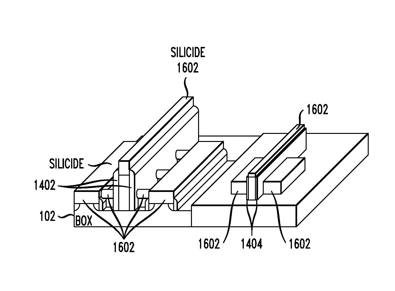
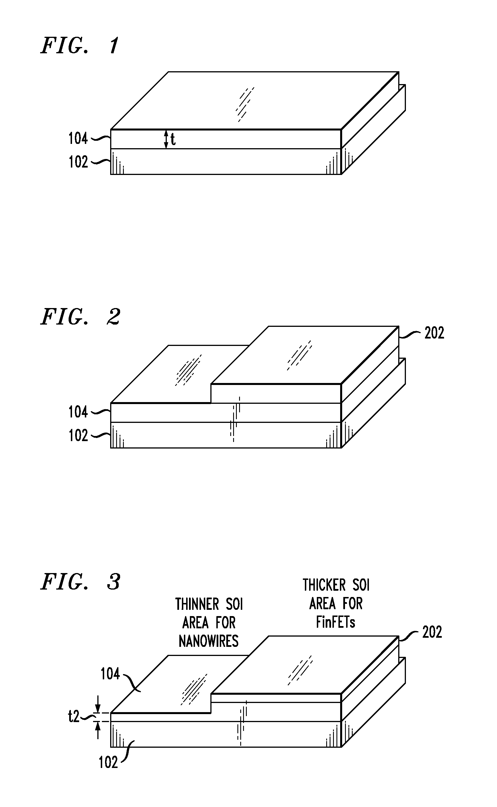
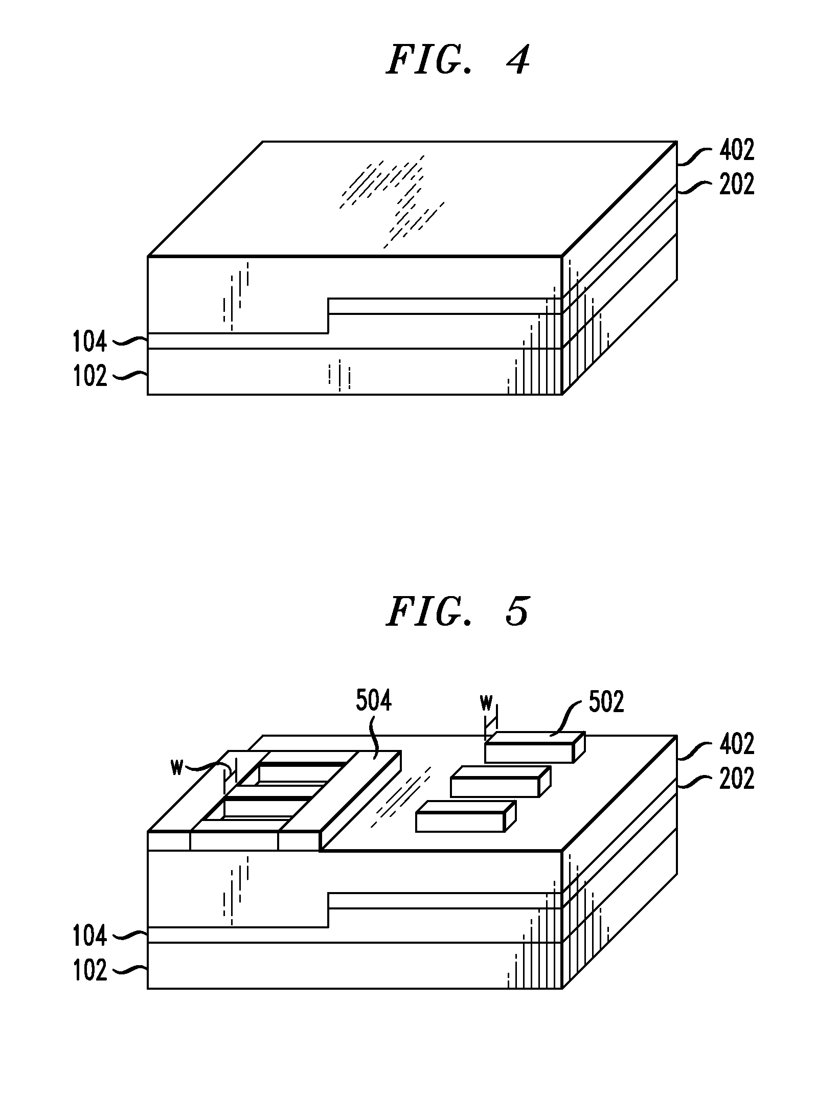
[0026]FIGS. 1-16 are diagrams illustrating an exemplary methodology for fabricating a complementary metal-oxide semiconductor (CMOS) circuit. The CMOS circuit will include an n-type field-effect transistor (NFET) device and a p-type FET (PFET) device. In the example now provided, the NFET device will employ a nanowire FET architecture and the PFET will employ a finFET architecture.

[0027]The fabrication process begins with a semiconductor-on-insulator (SOI) wafer. See FIG. 1. An SOI wafer typically includes a layer of a semiconductor material (also commonly referred to as a semiconductor-on-insulator layer or SOI layer) separated from a substrate by an insulator. When the insulator is an oxide (e.g., silicon dioxide (SiO2)), it is commonly referred to as a buried oxide, or BOX. According to the present techniques, the SOI layer will serve as an active layer of the device in which the nanowires and fins will be patterned. Thus, the SOI layer will be referred to herein as an active lay...


PUM


Abstract

Hybrid nanowire FET and FinFET devices and methods for fabrication thereof are provided. In one aspect, a method for fabricating a CMOS circuit having a nanowire FET and a finFET includes the following steps. A wafer is provided having an active layer over a BOX. A first region of the active layer is thinned. An organic planarizing layer is deposited on the active layer. Nanowires and pads are etched in the first region of the active layer using a first hardmask. The nanowires are suspended over the BOX. Fins are etched in the second region of the active layer using a second hardmask. A first gate stack is formed that surrounds at least a portion of each of the nanowires. A second gate stack is formed covering at least a portion of each of the fins. An epitaxial material is grown on exposed portions of the nanowires, pads and fins.

Description

FIELD OF THE INVENTION[0001]The present invention relates to integrated circuits, and more particularly, to hybrid nanowire field effect transistor (FET) and FinFET devices and methods for fabrication thereof.BACKGROUND OF THE INVENTION[0002]Complementary metal-oxide semiconductor (CMOS) circuits typically include a combination of n-type and p-type field effect transistor (FET) devices. Each FET device includes a source, a drain and a channel between the source and the drain. A gate electrode over and / or surrounding the channel regulates electron flow between the source and the drain.[0003]As feature sizes of CMOS circuits get increasingly smaller (commensurate with current technology) a number of challenges arise. For instance, scaling brings about issues related to electrostatics and mobility degradation in CMOS devices. A finFET architecture offers increased scaling opportunities beyond that attainable with planar devices. See, for example, B. Yu et al., “FinFET Scaling to 10 nm ...

Claims


Application Information

Patent Timeline
Patent Type & Authority Patents(United States)
IPC IPC(8): H01L27/12H01L21/8238
CPCB82Y10/00B82Y40/00H01L29/66469H01L29/0673H01L29/78696H01L21/845H01L27/1211H01L29/42392H01L21/3247
Inventor BANGSARUNTIP, SARUNYACHANG, JOSEPHINE B.CHANG, LELANDSLEIGHT, JEFFREY W.
Owner INT BUSINESS MASCH CORP
Why Eureka
Try Eureka