Optical excitation/detection device and method for making same using fluidic self-assembly techniques

a technology of optical excitation/detection and fluid self-assembly, which is applied in the direction of material analysis, radiological control devices, instruments, etc., can solve the problems that standard solid-state light emitting devices (like leds) are difficult to incorporate onto a cmos detector array

Inactive Publication Date: 2004-11-11
SANOFI AVENTIS DEUT GMBH
View PDF2 Cites 239 Cited by
  • Summary
  • Abstract
  • Description
  • Claims
  • Application Information

AI Technical Summary

Problems solved by technology

For example, standard solid state light emitting devices (like LEDs) are difficult to incorporate onto a CMOS detector array because the process for solid state LED photoemitter fabrication is incompatible with the CMOS fabrication process used to form the photodetectors.

Method used


Image

  • Optical excitation/detection device and method for making same using fluidic self-assembly techniques
  • Optical excitation/detection device and method for making same using fluidic self-assembly techniques
  • Optical excitation/detection device and method for making same using fluidic self-assembly techniques

Examples


Embodiment Construction

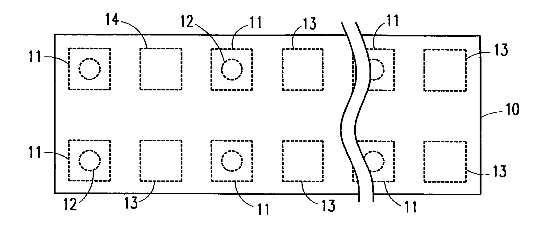
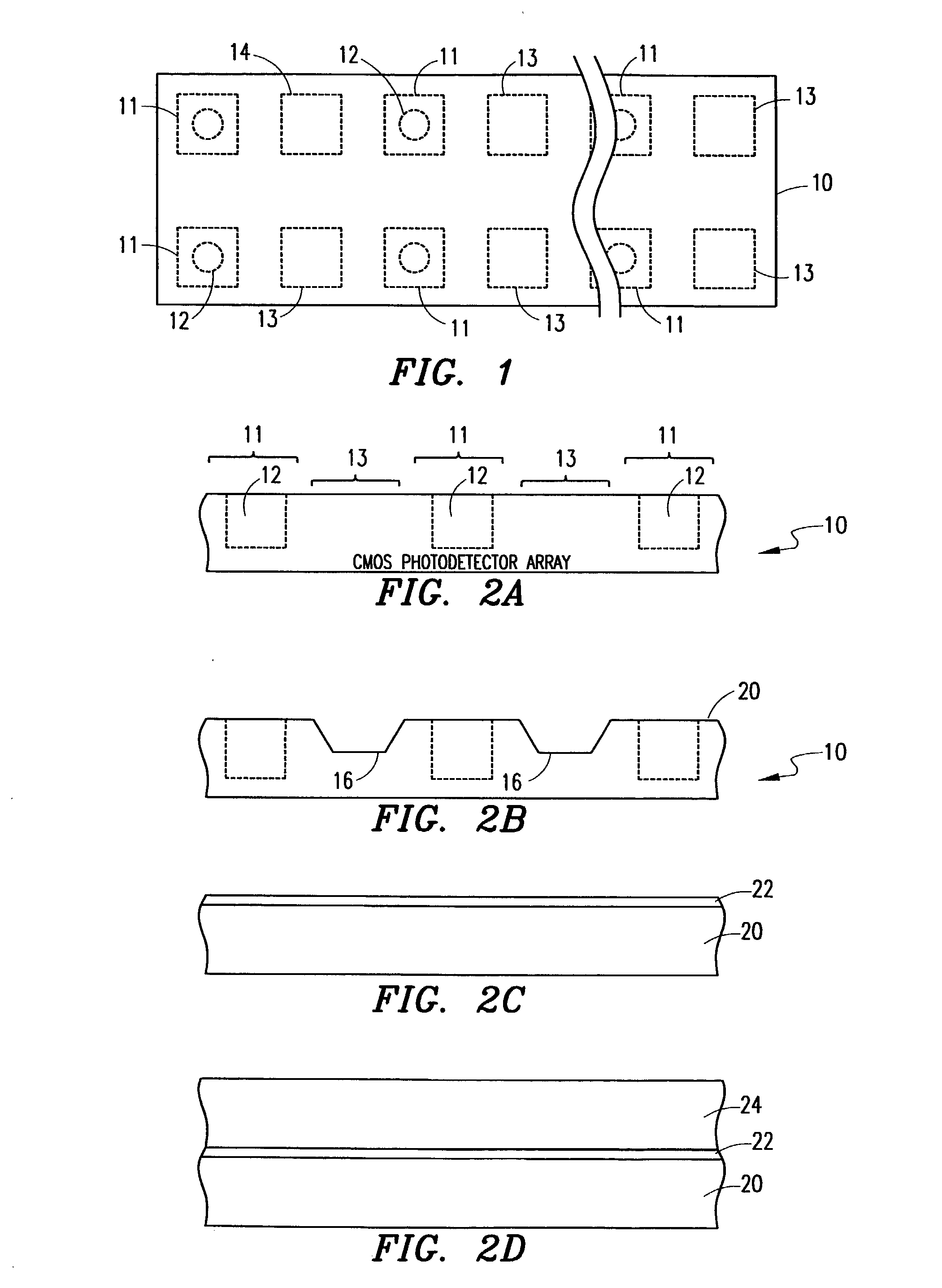
[0012] Reference is now made to FIG. 1 wherein there is shown a top view of a complementary metal oxide semiconductor (CMOS) photodetector array 10. It will be recognized by those skilled in the art that the features illustrated in FIG. 1 are not necessarily drawn to scale and that the size of certain features, dimensions, and the like, may be exaggerated to ease illustration and understanding. The CMOS array 10 is fabricated using conventional complementary metal oxide semiconductor fabrication techniques and includes an arrayed plurality of photoreceptor areas 11 and an arrayed plurality of photoemitter areas 13. Within each photoreceptor area 11, the CMOS fabrication process is used to form an integrated photoreceptor 12 (also referred to as a photodiode). Examples of such photoreceptors 12 include p-i-n diodes, avalanche photodiodes, charge coupled devices, or the like Associated circuitry (not specifically illustrated) for the photoreceptors 12 (for example, biasing circuits, f...


PUM

PropertyMeasurementUnit
sizeaaaaaaaaaa
semiconductoraaaaaaaaaa
areaaaaaaaaaaa

Abstract

The disclosure is directed toward an optical excitation / detection device that includes an arrayed plurality of photodetectors and separately formed photoemitters, as well as a method for making such a device. A CMOS fabricated photodetector array including a plurality of individual photoreceptors is selectively etched back between photoreceptor locations to reveal a plurality of recessed regions having a certain geographic profile. A plurality of semiconductor blocks, each having light emitting capability and each having a certain geometric profile that is complementary in size and shape to the certain geometric profile of the recessed regions, are separately fabricated. These blocks are included within a fluid to form a slurry. The slurry is then flowed over the CMOS fabricated photodetector array in accordance with a fluidic self-assembly technique, and the included semiconductor blocks are individually deposited within each of the plurality of recessed regions in the CMOS fabricated photodetector array. The deposited blocks are then attached within the recessed regions to form the optical excitation / detection device from an arrayed plurality of photodetectors and separately formed photoemitters.

Description

[0001] 1. Technical Field of the Invention[0002] The present invention relates to a device for optical excitation / detection including an arrayed plurality of photodetectors and photoemitters and, in particular, to such a device manufactured using fluidic self-assembly techniques.[0003] 2. Description of Related Art[0004] Detector arrays (i.e., devices comprising an arrayed plurality of photodetectors) can be fabricated using well known complementary metal oxide semiconductor (CMOS) fabrication techniques. Such arrays are typically of very high quality, exhibit low noise and are inexpensive to produce What is lacking with conventional CMOS fabrication techniques for such devices is a way of easily incorporating a plurality of light emitting devices (for example, light emitting diodes (LEDs), laser diodes, or other type photoemitters) into the CMOS array detector device. For example, standard solid state light emitting devices (like LEDs) are difficult to incorporate onto a CMOS detec...

Claims


Application Information

Patent Timeline
Patent Type & Authority Applications(United States)
IPC IPC(8): H01L21/98H01L25/16H01L27/146H01L31/00H01L31/12
CPCH01L24/95H01L25/167H01L25/50H01L27/14683H01L31/125H01L2224/95085H01L2924/01013H01L2924/01015H01L2924/01027H01L2924/01049H01L2924/10158H01L2924/01033H01L2924/12041H01L2924/12042H01L2924/12043H01L2224/95136H01L2224/95101H01L2924/00
Inventor KING, DAVID ANDREWPITTARO, RICHARD J.RANA, SHAHIDAVERDONK, EDWARDSTAWITCKE, FREDERICK A.PERING, RICHARD D.
Owner SANOFI AVENTIS DEUT GMBH
Why Eureka
Try Eureka