First of all, many analog and power ICs are connected directly to the battery or power input of a product and are therefore subjected to a full range of potential over-
voltage and
noise conditions.
Furthermore, the inputs to analog ICs often are themselves analog signals which may include
noise mixed into the
signal being monitored or detected.
These loads may include inductors or motors, causing the output pin of the IC to exceed the supply
voltage or go below ground potential, and may result in the forward biasing of PN junctions leading to undesirable
parasitic bipolar transistor conduction.
But in most instances digital ICs use fabrication processes optimized to produce transistors that consume the smallest possible area, even if the ideality or performance of the semiconductor devices must suffer in order to reduce area.
Most of these processes require a complex process flow to achieve isolation between devices, especially when NPN or PNP bipolars are included.
The process is complicated by the fact that the buried layer
implant must be diffused well away from the surface prior to epitaxial growth to avoid unwanted and excessive updiffusion of the buried layer into the epitaxial layer.
There are numerous aspects of this standard fabrication process that impose limitations on the characteristics and variety of devices that can be formed in the epi layer.
Obviously, this limits the horizontal proximity of the devices to each other, since a certain horizontal spacing must be provided between the implants in anticipation of the lateral spreading that will occur during the anneal.
This limits the packing density of the devices on the
wafer.
Second, since all of the devices in a given
wafer are necessarily exposed to the same thermal processes, it becomes difficult to fabricate devices having diverse, preselected electrical characteristics.
For example, Device A may require an anneal at 900° C. for one hour in order to achieve a desired electrical characteristic, but an anneal at 900° C. for one hour may be inconsistent with the electrical characteristics required for Device B, moving or redistributing the dopants in an undesirable way.
Once a
dopant has been implanted, it will be subjected to whatever “thermal budget” is applied to the
wafer as a whole thereafter, making
dopant redistribution unavoidable.
Such retrograde profiles are not possible using an all-diffused process.
Such profiles are not possible using an all-diffused process.
Attempts have been made to produce such flat profiles using multiple buried
layers alternating with multiple epitaxial depositions, but these processes are prohibitively expensive since
epitaxy is inherently a slower, more expensive process step than other fabrication operations.
Since thicker
layers are needed to support higher voltage isolated devices, there is a severe penalty between the
voltage rating of a device and the wasted area needed to isolate it.
Larger die area results in fewer die per wafer, resulting in a more expensive die cost.
As explained previously, higher voltage devices requires deeper, less area-efficient isolation diffusions.
These thick, wide-isolation diffusions are then required even in the lower voltage sections of the
chip,
wasting even more area.
Sixth, many IC processes do not have the capability to integrate a voltage independent
capacitor like poly-to-poly, poly-to-
metal, or
metal to poly, nor do they contain a high
sheet resistance material for high value resistors.
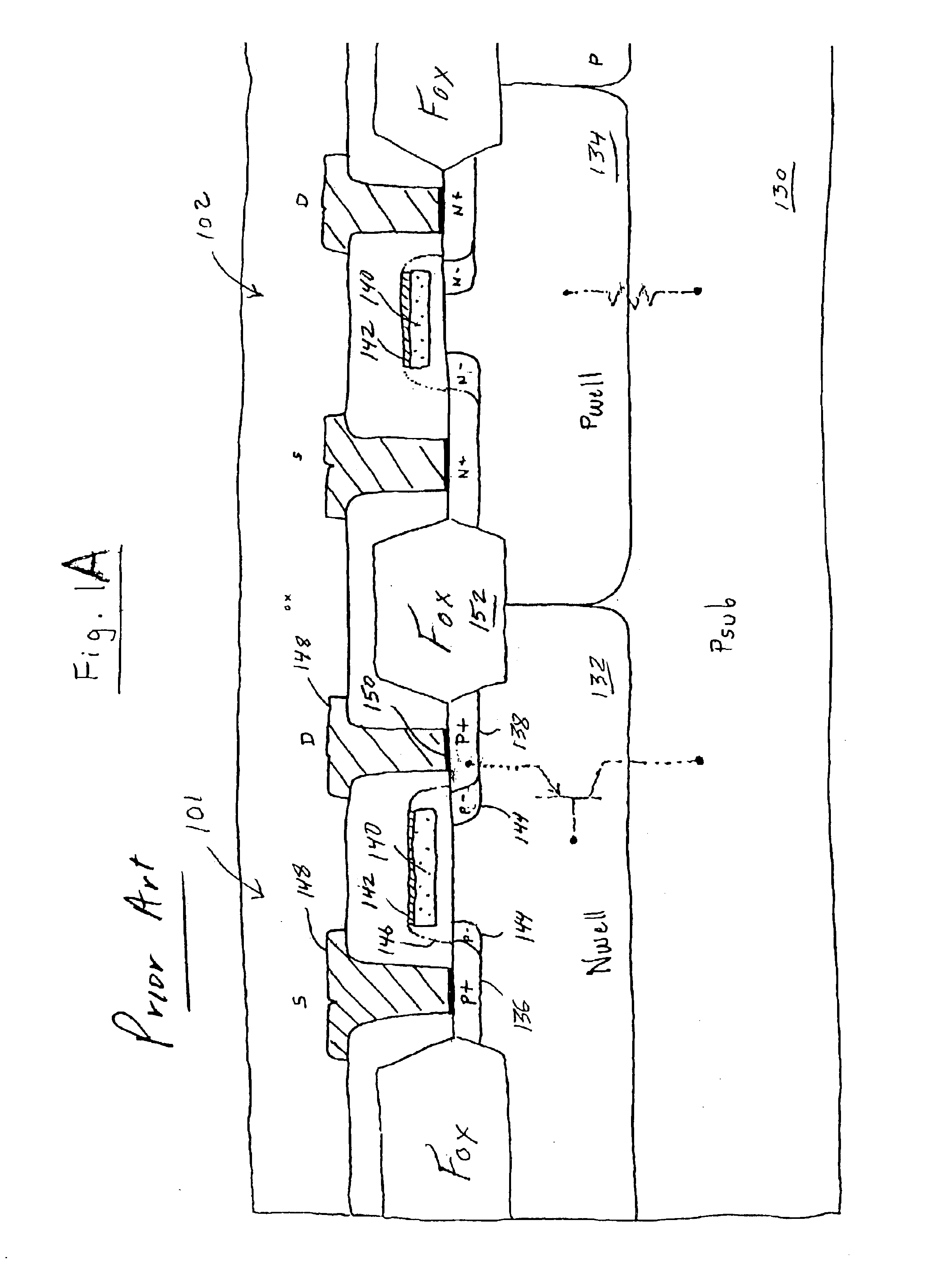
A problem with this device is that NMOS 102 is not isolated from the P substrate 130, since there is no PN junction between P substrate 130 and P well 134.
Since N well 132 has a limited amount of
doping present in such well region, the PMOS may not always operate in an ideal manner, especially due to parasitic bipolar conduction.
There the body of NMOS 102 is resistively tied to ground and the source is typically shorted to ground and the device therefore cannot be isolated.
As a result, the devices cannot be floated in circuit that is not reasonably near the ground potential, without risk of the PNP conducting or exhibiting
snapback breakdown, especially at high temperatures.
Where there are parasitic bipolar transistors, or where
impact ionization occurs, so many carriers are generated the voltage collapses or “snaps back” after breakdown (curve A2) and if the current rises too much the device will be destroyed.
Hot carriers are generated by the channel current through the device and these hot carriers can cause the device to snap back in what is sometimes referred to as a
safe operating area (SOA) failure.
The fact that the
doping concentrations and profiles cannot be controlled very accurately, because the dopants are being thermally diffused, makes these problems worse, especially considering that
Gaussian dopant profiles have their highest concentrations at the
silicon surface, where the electric fields are also highest.
If this happens the device will most likely be destroyed.
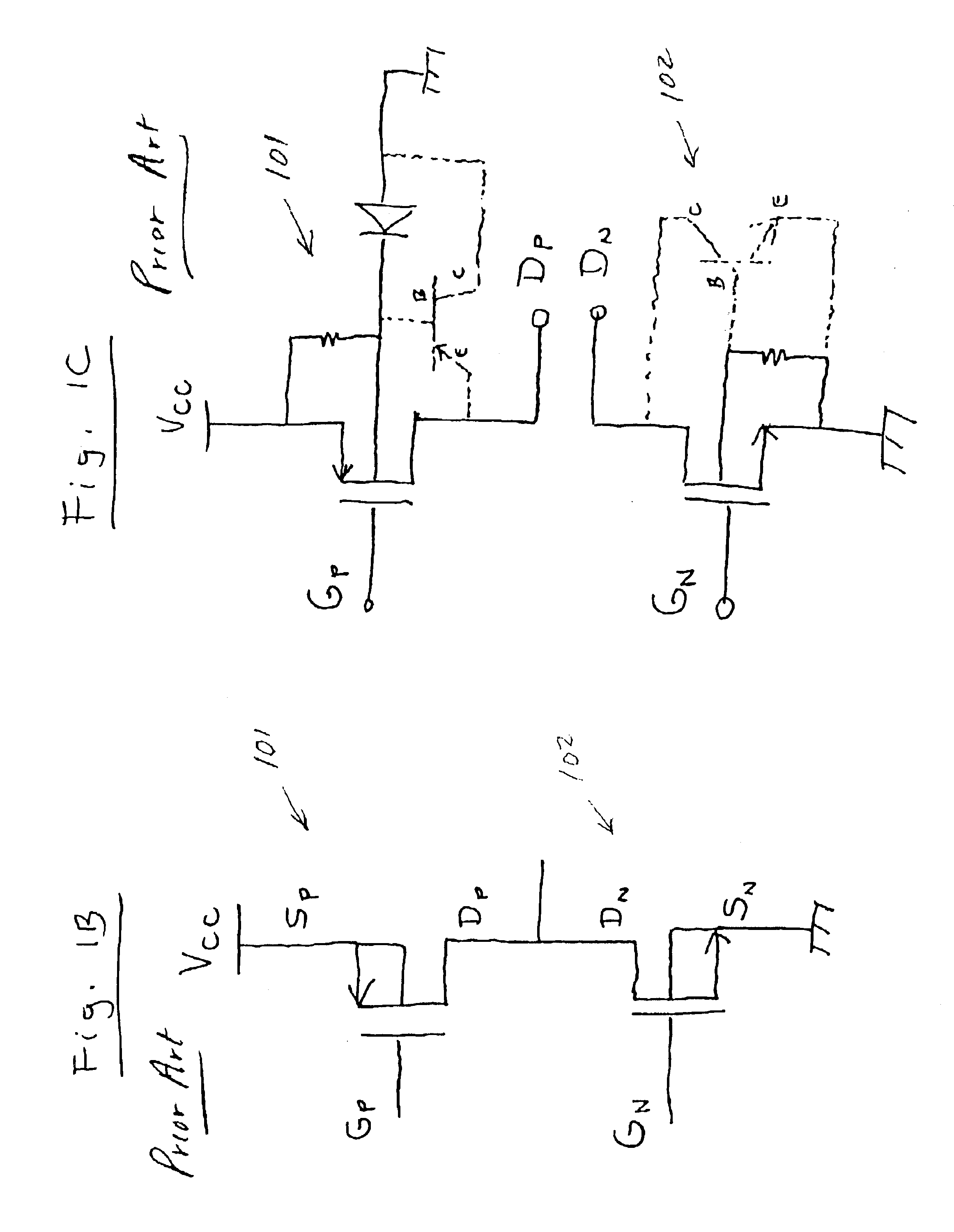
Probably the biggest single problem with PMOSs 101, 103 is that they are not floating, meaning they cannot be biased at a high N well-to-P substrate potential without snapping back.
Similarly, one of the biggest problems with NMOSs 102, 104 is that they are not floating, meaning their body connection cannot be biased above the substrate potential at all.
This limits greatly the types of circuits in which they can be used.
One problem with this structure is that it requires long diffusions.
The long anneal required to diffuse P body 182, however, would render useless any threshold adjust
implant that was previously performed in the
CMOS pair.
The only way to avoid this problem would be to deposit the gate 186 of lateral DMOS before the gates 188 of the CMOS, but this would add considerable complexity to the process.
One could use a 0.35 μm process to fabricate this structure but the number of masking steps could become excessive.
Moreover, the effort to reduce the size of CMOS devices and the resulting benefit in reduced die size are mostly lost when the large wasted area of isolation diffusions 180 is considered.
To keep this resistance within acceptable limits N+ sinkers must be positioned periodically and frequently between the DMOSs, and this reduces the packing density of the chip.
A greater vertical
diffusion means a greater horizontal
diffusion, so this further increases the size of the device.
This is a highly variable process that is difficult to control.
It is difficult to guarantee good alignment with this procedure, requiring extra spacing to be included in the design rules of a device and
wasting silicon area.
Such a limitation imposes many restrictions in the
device type and device optimization possible.
One cannot fabricate regions having predetermined yet arbitrary, non-
Gaussian dopant profiles.
For example, a retrograde profile having a higher subsurface concentration than its
surface concentration cannot be performed using purely diffused techniques.
Such diffusions (and diffusions in general) are difficult to accurately control, and the actual results may vary widely from what is desired especially when the variability from wafer-to-wafer (from a single wafer batch ) and variability from wafer-batch to wafer-batch (so called “run-to-run variation) are considered.
The variability comes from poor
temperature control and from dopant segregation occurring during oxidation.
Moreover, the diffusions, while intended primarily to introduce dopants deeper into the substrate, also spread the dopants laterally, and this increases the size of the devices, in some cases by substantial amounts.
Variability in epitaxial thickness and in concentration compound device optimization, and the epitaxial process necessarily occurs at a high temperature, typically over 1220° C. Such high-temperature
processing causes unwanted updiffusion of the substrate in some regions of an IC, and of buried
layers in other regions.
Isolating a thicker epitaxial layer requires even longer
diffusion times for the isolation diffusion structure, leading to excessively wide features.
This penalty leads to poor packing densities for
low voltage on-chip devices, all because of one higher voltage component.
If the higher voltage device is not used, the wasted area lost to
high voltage isolation (and related design-rule spacing) cannot be reclaimed without re-
engineering the entire process and affecting every component in the IC.
Such a process is not modular, since the addition or removal of one component adversely affects all the other
integrated devices.

