

Three dimensional integrated circuit and method of design
a three-dimensional integrated circuit and design method technology, applied in the field of design and fabrication of integrated circuits, can solve the problems of increasing chip power consumption, increasing cooling and packaging costs, and always being limited by those minimum dimensions, so as to improve ic chip density and improve ic chip functionality without complicating ic chip design, and without impairing chip performance
- Summary
- Abstract
- Description
- Claims
- Application Information
AI Technical Summary
Benefits of technology
Problems solved by technology
Method used
Image

Examples
Embodiment Construction
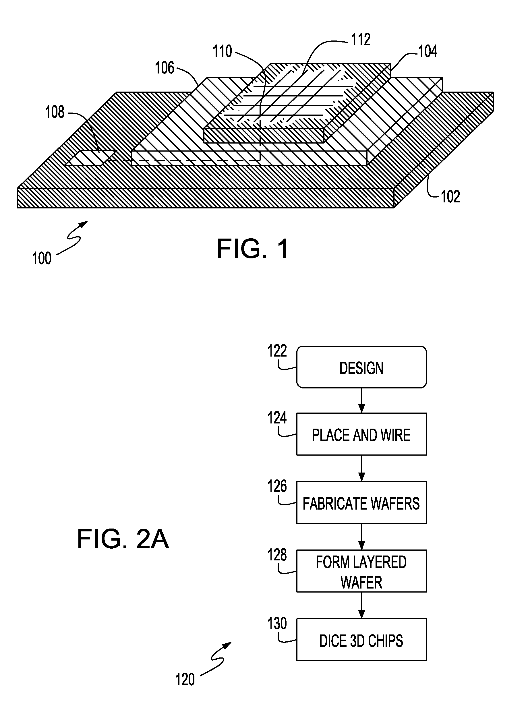
[0020] Turning now to the drawings and, more particularly, FIG. 1 shows an example of a preferred embodiment three dimensional (3D) integrated circuit (IC) chip 100 formed according to the present invention. In this example, a first layer of circuits 102 supports a second layer of circuits 104, e.g., where the first layer 102 is a synchronous logic or pipeline layer and the second layer 104 includes a clock distribution (clock tree) for the first layer 102. It should be noted that as referred to herein a layer of circuits is a device structure or circuit wherein complete individual active and / or passive devices are contained and, further, may be wired together. Thus, circuits in a layer of circuits may include capacitors, such as decoupling capacitors, inductors, resistors and etc. In this example, the layers of circuits 102, 104 are connected together by an optional third layer of circuits 106 sandwiched therebetween, which is a layer of wires in this example. Circuit elements 108,...
PUM
 Abstract
Description
Claims
Application Information