Layer transfer process and functionally enhanced integrated circuits produced thereby

a layer transfer and integrated circuit technology, applied in the direction of semiconductor devices, electrical devices, semiconductor/solid-state device details, etc., can solve the problems of high cost, high cost, time-consuming, etc., and achieve the effects of enhancing functionality, wide applicability, and low cost of ownership

Inactive Publication Date: 2010-04-01
LINKEDIN
View PDF9 Cites 430 Cited by
  • Summary
  • Abstract
  • Description
  • Claims
  • Application Information

AI Technical Summary

Benefits of technology

[0012]In particular, it is an object of this invention to provide a supporting structure for integrated planar ICs for high frequency and high speed computing applications. It is further an object of this invention to leverage the know-how of the layer transfer technology to form a complete high density interconnect structure with integrated functional components such as ground connections / networks and power planes providing thermal and electrical “drops” or conducting elements. Finally, this invention provides a low cost of ownership scheme to create integrated structures with enhanced functionality by extending the art in existing semiconductor technology as it is based on wafer level technology.
[0013]This invention is of wide applicability since it provides a technique and structure in which functional elements such as wiring levels are added in the form of networks or planes underneath a device layer, more particularly a semiconductor device layer. These added elements enable a new level of electrical as well as thermal components to be easily used to enhance CMOS and other technologies. Additional functional elements to enable MEMS, optoelectronics and biotechnology can also be added above or below the device layer to achieve hybrid multifunctional systems currently not feasible by conventional art of fabrication in CMOS technology.

Problems solved by technology

Interconnect challenges for future microprocessors and other high performance chips arise from the continued push to lower k-effective of interlevel dielectric materials, higher aspect ratio for all wiring levels, and increasing number of metalization layers.
However, as future interconnects shrink in dimension to allow gigascale integration, the signal delay and the signal fidelity problems associated with the interconnects become significant limiters of the overall system performance (e.g., maximum supportable chip clock frequencies or via blockage due to the need of a large number of vias to connect the multiplicity of wiring levels).
Since changes in system architectures of the planar CMOS IC technology do not achieve a significant performance yield increase per year, and further increase of the number of the interconnect levels raises significant reliability questions, new solutions become a necessity if significant improvements of planar CMOS technology are to be achieved in future IC generations.
This solution comes at a high cost and is very time consuming as every new generation of products has to be redesigned and verified.
Changes in architecture are difficult as they encompass a span of many critical building blocks including: memory and logic, routing, hierarchy, etc.
Therefore, it has been realized that there will be a slow down in the rate of performance improvements for new generations relative to the famous Moore's law of microprocessors if one were to depend on planar architecture alone.

Method used


Image

  • Layer transfer process and functionally enhanced integrated circuits produced thereby
  • Layer transfer process and functionally enhanced integrated circuits produced thereby
  • Layer transfer process and functionally enhanced integrated circuits produced thereby

Examples


Embodiment Construction

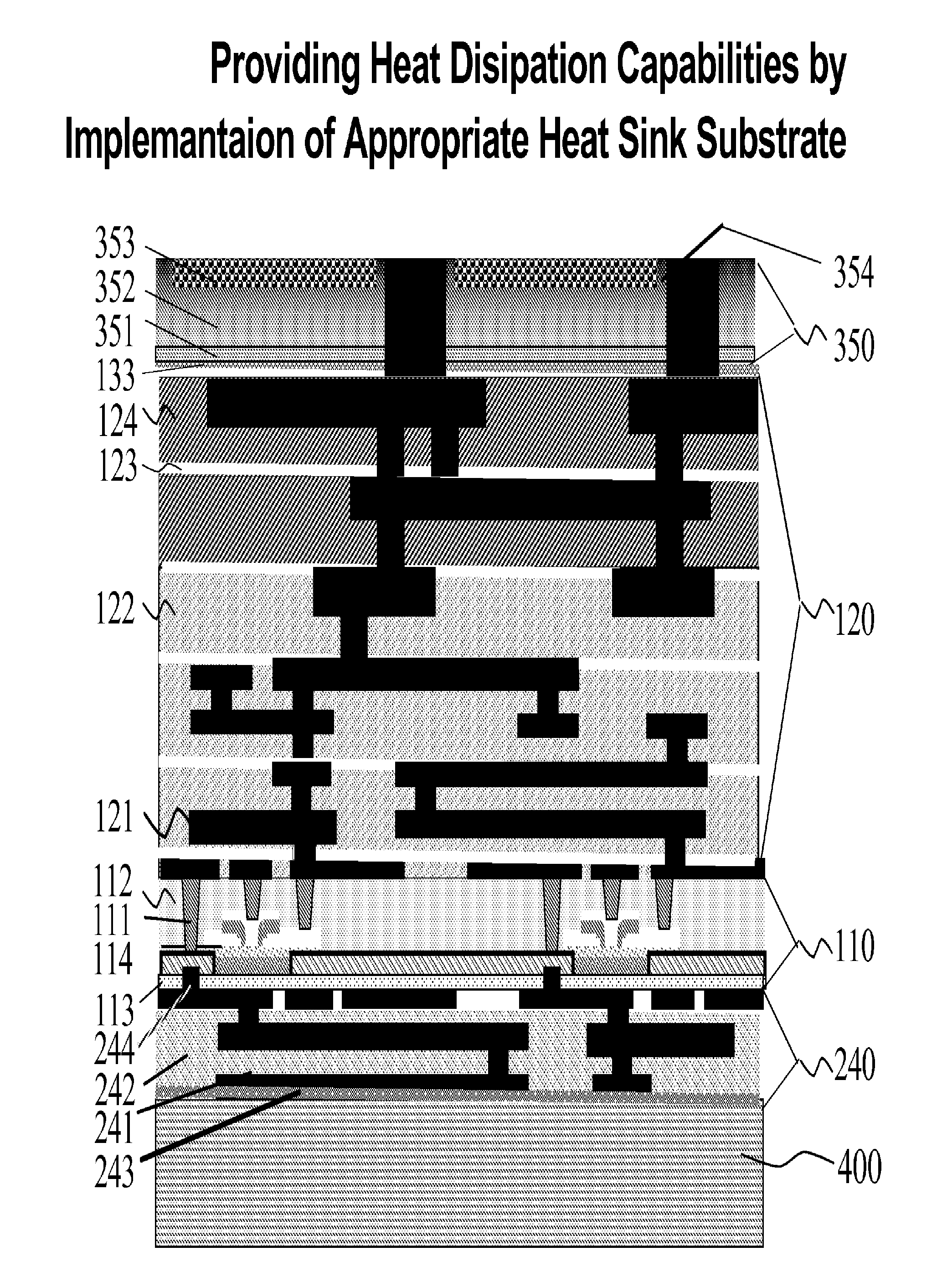
[0027]The present invention is based on the creation of enhanced 2D CMOS IC structure with functional elements on both sides BEOL IC solution enables improved performance of this novel structure, adds functionality and simplifies processing issues related to multilevel builds by utilizing layer transfer and sequential layer wise build approaches as and where appropriate.

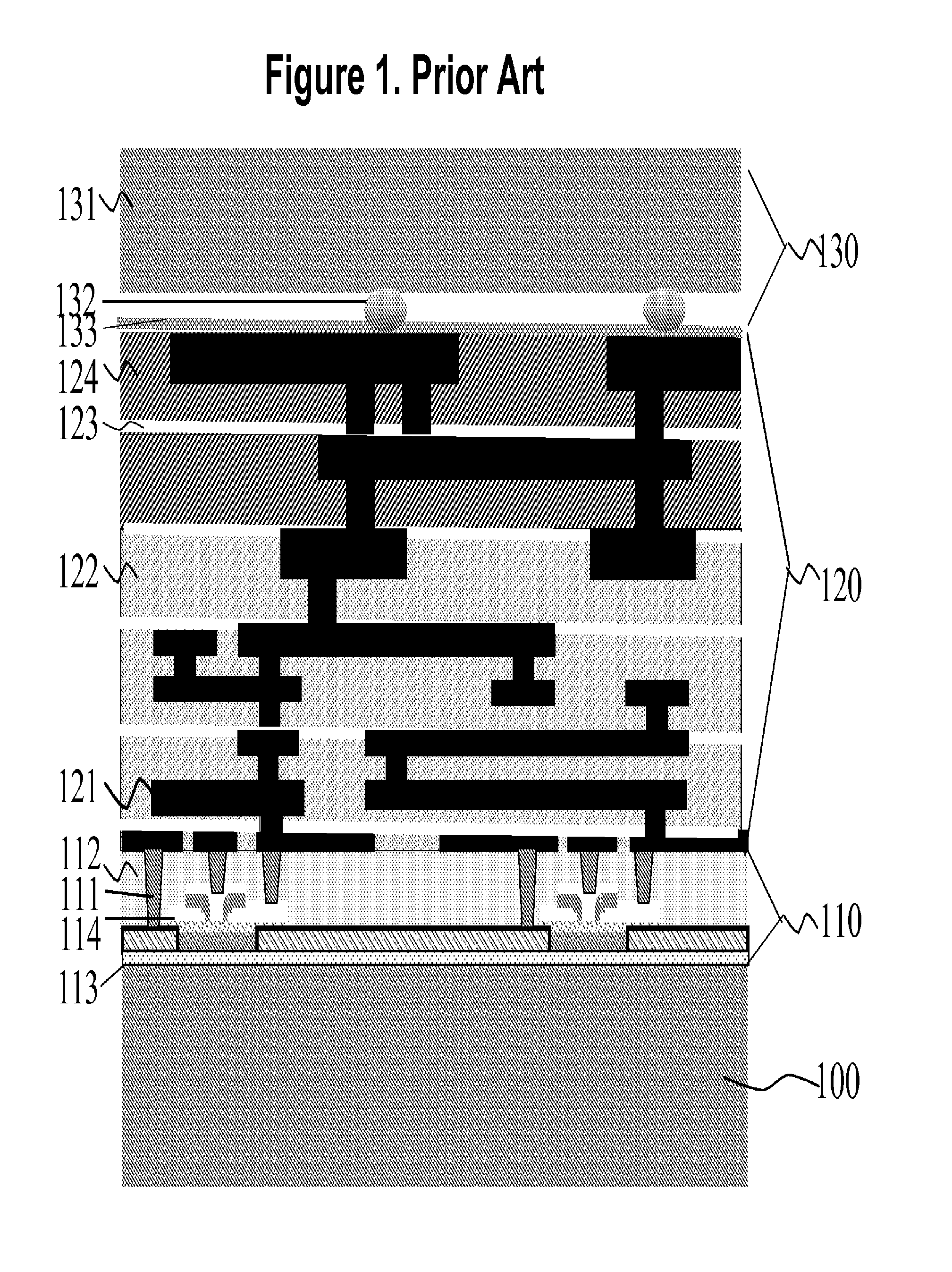
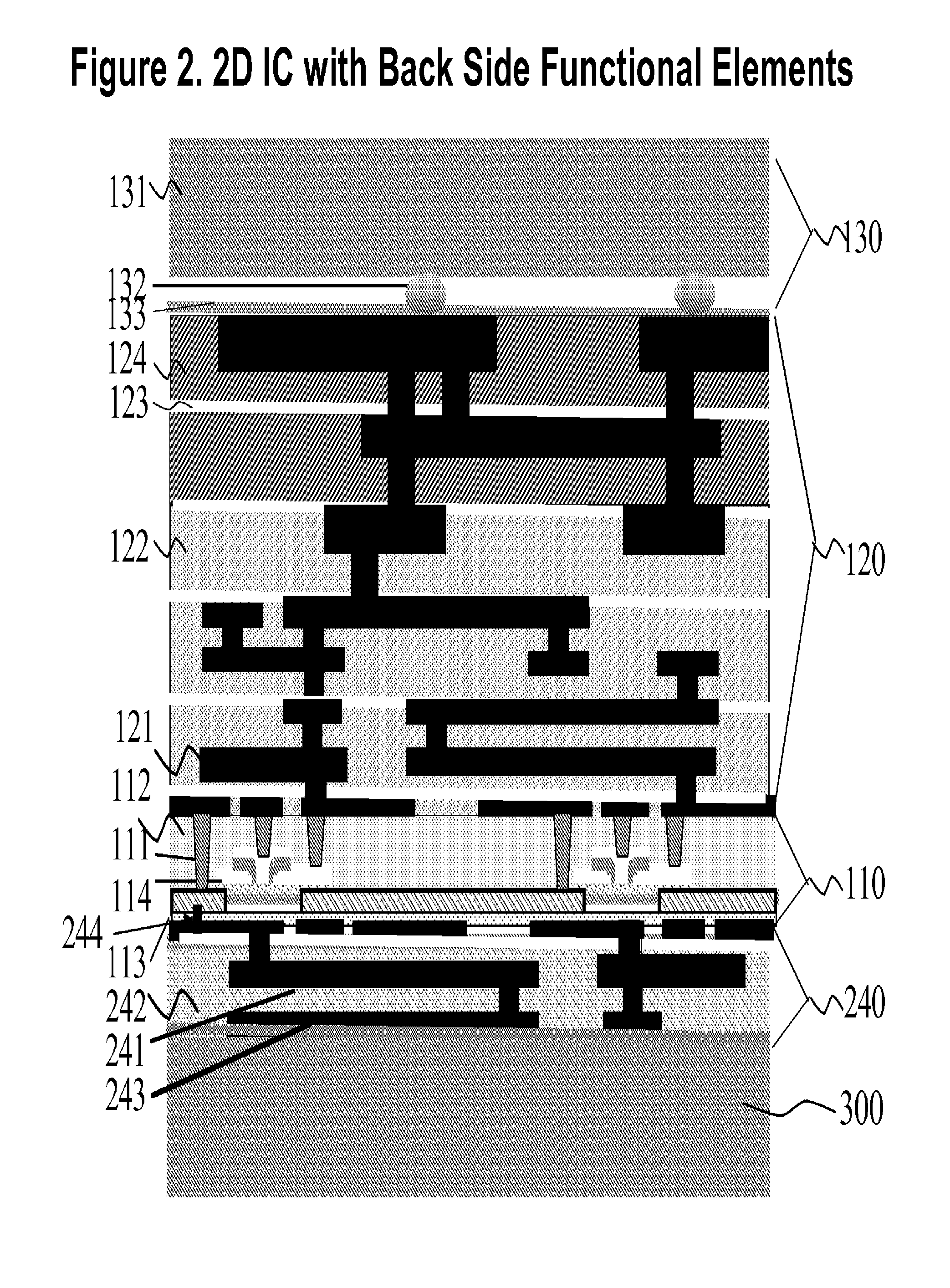
[0028]In the first embodiment of the present invention, a CMOS technology structure (see FIG. 1) with its problems related to the via blockage, multi-layer wiring, etc., is transformed into an enhanced planar IC CMOS structure based on creation of a wiring scheme that is disposed on both sides of the device layer (see FIG. 2). This is distinct from the structure illustrated in FIG. 1 which can be described as follows: In FIG. 1 the FEOL structure [110] is fabricated on the substrate [100] and interconnected on the top using BEOL levels [120]. FEOL structure [110] would include the various transistors and the associat...


PUM


Abstract

A structure for a semiconductor components is provided having a device layer sandwiched on both sides by other active, passive, and interconnecting components. A wafer-level layer transfer process is used to create this planar (2D) IC structure with added functional enhancements.

Description

[0001]This application is a divisional application of co-pending application Ser. No. 11 / 746,680 filed May 10, 2007 of which the benefit of the earlier filing date is claimed.FIELD OF THE INVENTION [0002]The present invention relates to the three dimensional integration of circuit components into functionally enhanced structures using wafer-level layer transfer process based on the incorporation of added functional elements such as new wiring and placement schemes for interconnection of semiconductor components.BACKGROUND OF THE INVENTION[0003]Interconnect challenges for future microprocessors and other high performance chips arise from the continued push to lower k-effective of interlevel dielectric materials, higher aspect ratio for all wiring levels, and increasing number of metalization layers. At this point the back-end-of-the-line (BEOL) consists of as many as ten metalization levels that contain wires to provide interconnections for signal, clock, power, repeaters, devices, d...

Claims


Application Information

Patent Timeline
Patent Type & Authority Applications(United States)
IPC IPC(8): H01L21/50H01L21/768
CPCH01L21/2007H01L21/768H01L21/84H01L23/3735H01L27/0688H01L2924/0002H01L27/1203H01L2924/00
Inventor FURMAN, BRUCE K.PURUSHOTHAMAN, SAMPATHSANKARAPANDIAN, MUTHUMANICKAMTOPOL, ANNA
Owner LINKEDIN
Why Eureka
Try Eureka