Frame buffer pixel circuit for liquid crystal display

a liquid crystal display and frame buffer technology, applied in static indicating devices, non-linear optics, instruments, etc., can solve the problems of affecting the brightness and contrast ratio of related art frame buffer pixels, affecting the brightness and contrast ratio of related art, and affecting the brightness of related ar

Inactive Publication Date: 2005-06-28
DUKE UNIV +1
View PDF14 Cites 230 Cited by
  • Summary
  • Abstract
  • Description
  • Claims
  • Application Information

AI Technical Summary

Benefits of technology

[0013]It is another object of the claimed invention to provide an enhanced frame buffer pixel circuit that can achieve high contrast ratio and display high quality images with shorter writing time.
[0014]In the preferred embodiment of the frame buffer pixel circuit, two separate capacitors are utilized to yield higher contrast ratio by minimizing the induced charge during data writing or reading time, keeping the dark level at its lowest brightness and therefore saving data writing time. The capacitance of the separate capacitor does not depend on that of each other and, therefore, can be designed independently such that the time constant is long enough to hold the stored charge for one frame time. The capacitance of the separate capacitors is not voltage-dependent contrary to the gate capacitance. The lcd capacitor Clcd is directly driven by the power source, the current flowing into the lcd capacitor is controlled by the voltage level stored at the memory capacitor. Furthermore, there is no charge sharing between the memory capacitor Cmem and the lcd capacitor Clcd. There is charge induced only when data read signal is on, however the amount of charge induction is same for all data level. Thus the charge induction does not alter the gray level and the charge induced at the lcd capacitor can also be minimized by using minimum-sized transistor. In the preferred embodiment of the frame buffer pixel circuit, an analog to pulse width modulation (PWM converter can be put after the pixel electrode (i.e., lcd capacitor) Clcd. Specifically, a pixel capacitor Cpixel is preferably connected to a comparator with a reference voltage Vref to generate PWM pulses to drive binary displays such as ferroelectric liquid crystal displays and digital mirror displays (DMDs), reducing the sub-frame frequency significantly.

Problems solved by technology

However, even with a much larger Cmem memory capacitor, there is always some voltage drop due to the charge sharing effect.
That is, the remaining charge at the Clcd node from the previous image interferes with the new voltage that is written for a new image.
Due to these disadvantages, the related art frame buffer pixel provides poor brightness and contrast ratio.

Method used


Image

  • Frame buffer pixel circuit for liquid crystal display
  • Frame buffer pixel circuit for liquid crystal display
  • Frame buffer pixel circuit for liquid crystal display

Examples


Embodiment Construction

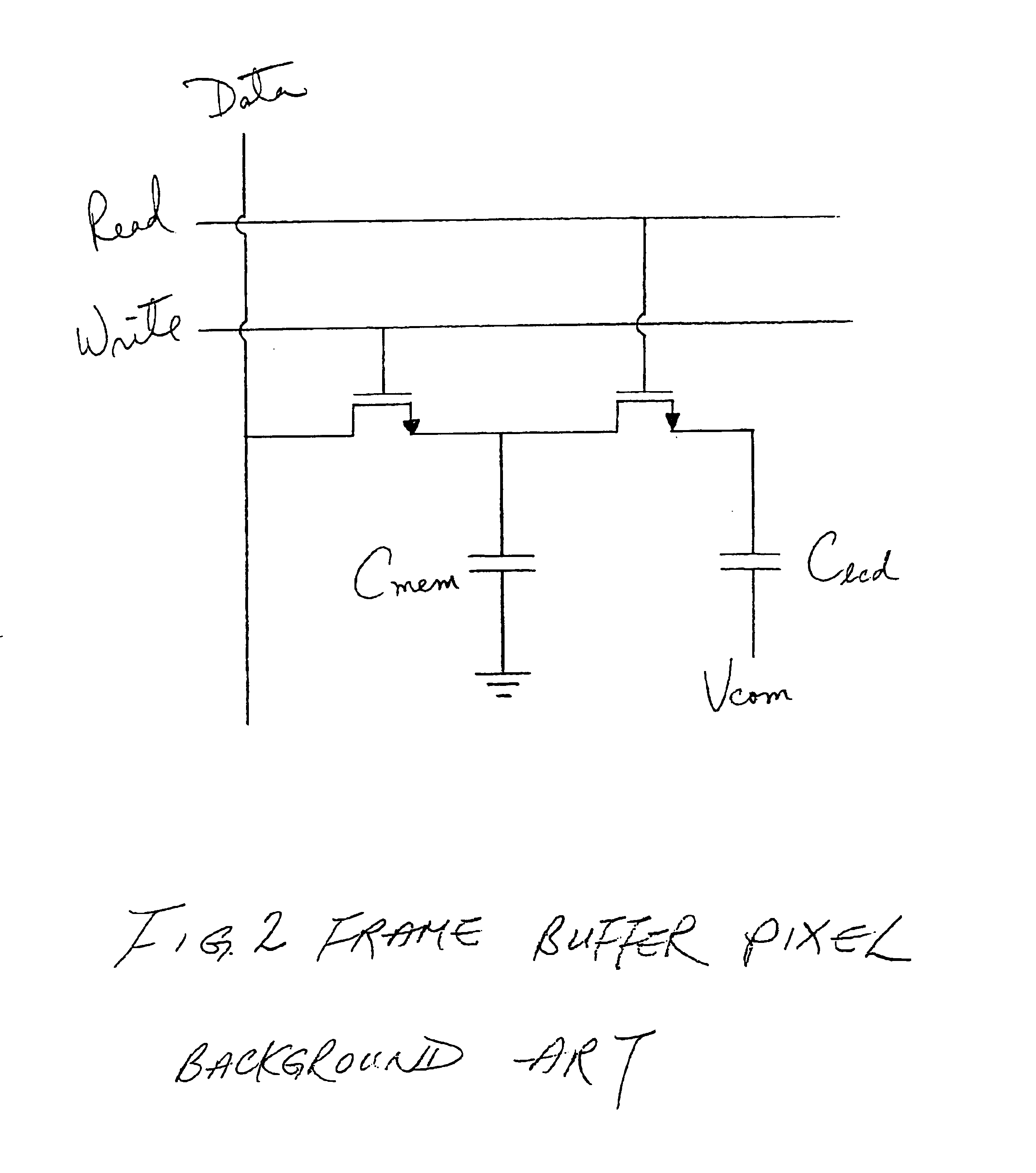
[0037]Preferred embodiments of the present invention will now be described with reference to the accompanying drawings. FIG. 6 shows a first refined frame buffer pixel circuit. In this refined frame buffer pixel circuit, a memory capacitor Cmem is put in the related art frame buffer pixel circuit of FIG. 4, eliminating the charge induction problem caused by the gate capacitance of transistor M3 with the Clcd capacitor, which forms an additional path to the ground. The image quality is greatly improved after the capacitor Cmem put in the related art frame buffet circuit and transistor M3 is preferably made from a minimum-sized transistor. Furthermore, as described below, the values of capacitors Cgs and Clcd can be optimized to achieve best image quality.

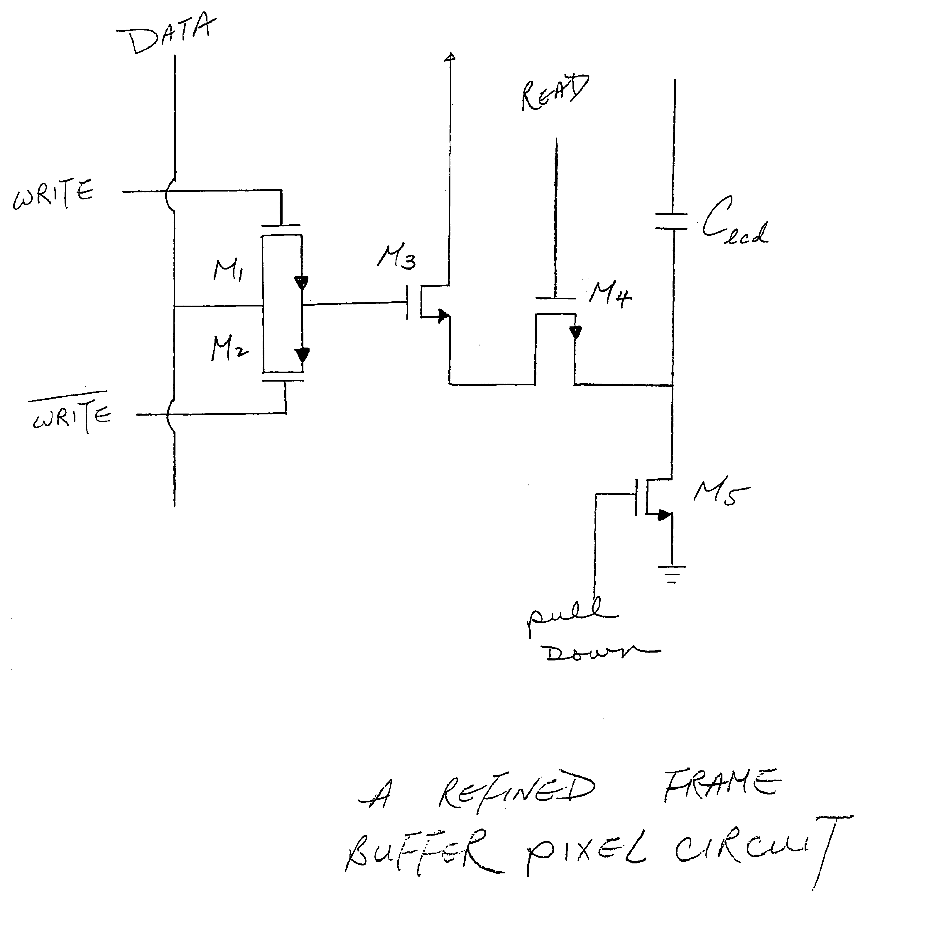
[0038]FIG. 7 shows a second refined frame buffer pixel circuit. In this second refined frame buffer pixel circuit, two field effect transistors (FETs), M1 and M2, are used as control or pass transistors. A pullup transistor M4 with a...


PUM


Abstract

An enhanced frame buffer pixel circuit with two control transistors and a separate capacitor put in as a memory capacitor before the memory transistor yields a high contrast ratio by removing induced charge and solving a charge sharing problem between the memory capacitor and the liquid crystal display (LCD) capacitor. The memory transistor may be made of either CMOS or PMOS. The frame buffer pixel can be used to drive binary displays which expresses ON and OFF only if a comparator is put in after the pixel electrode circuit to represent gray levels with reduced sub-frame frequency.

Description

BACKGROUND OF THE INVENTION[0001]1. Field of the Invention[0002]This invention relates to pixel circuits for display systems, and more particularly relates to a frame buffer pixel circuit for a liquid crystal display.[0003]2. Background of the Related Art[0004]FIG. 1 shows a related art display device 10. It includes a pixel circuit display panel 20 controlled by a display control circuit 30 having a frame memory 40. The related art pixel circuit display requires a grayscale representation of more than 8 bits per color, and an operating voltage low enough to enable a battery powered display device, such as a laptop computer or a personal digital assistant (PDA). The related art pixel circuit utilizes an address driver for address selection and a scan driver for image switching and reading cycles during displaying.[0005]FIG. 2 illustrates a related art early stage frame buffer pixel system for a liquid crystal display. Initially, a voltage proportional to the Data level is stored at ...

Claims


Application Information

Patent Timeline
Patent Type & Authority Patents(United States)
IPC IPC(8): G09G3/36G09G3/20
CPCG09G3/3648G09G3/2014G09G2300/0809G09G2320/0223G09G2300/0847G09G2310/0251G09G2310/0259G09G2300/0842
Inventor LEE, SANGROKMORIZIO, JAMES C.JOHNSON, KRISTINA M.
Owner DUKE UNIV
Why Eureka
Try Eureka