

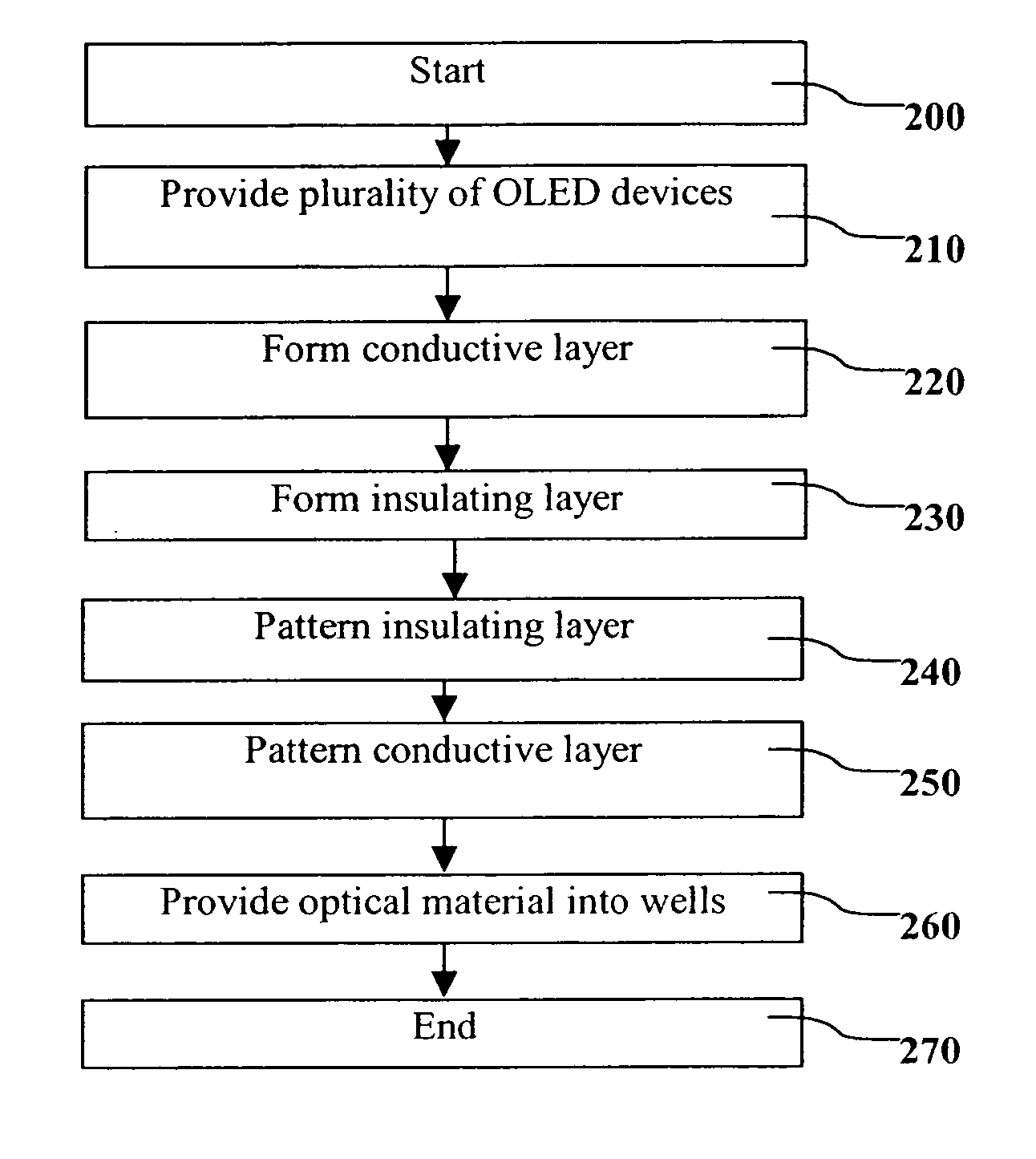
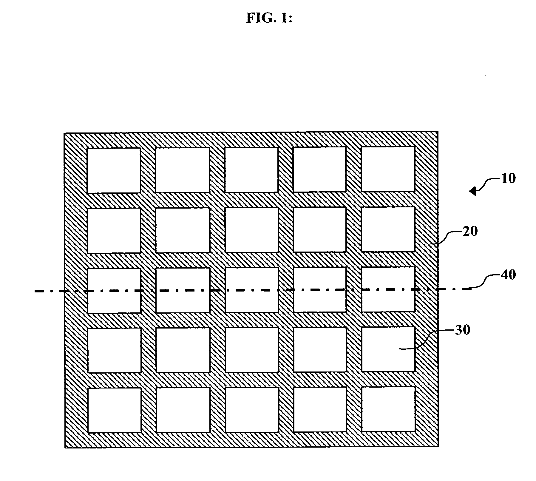
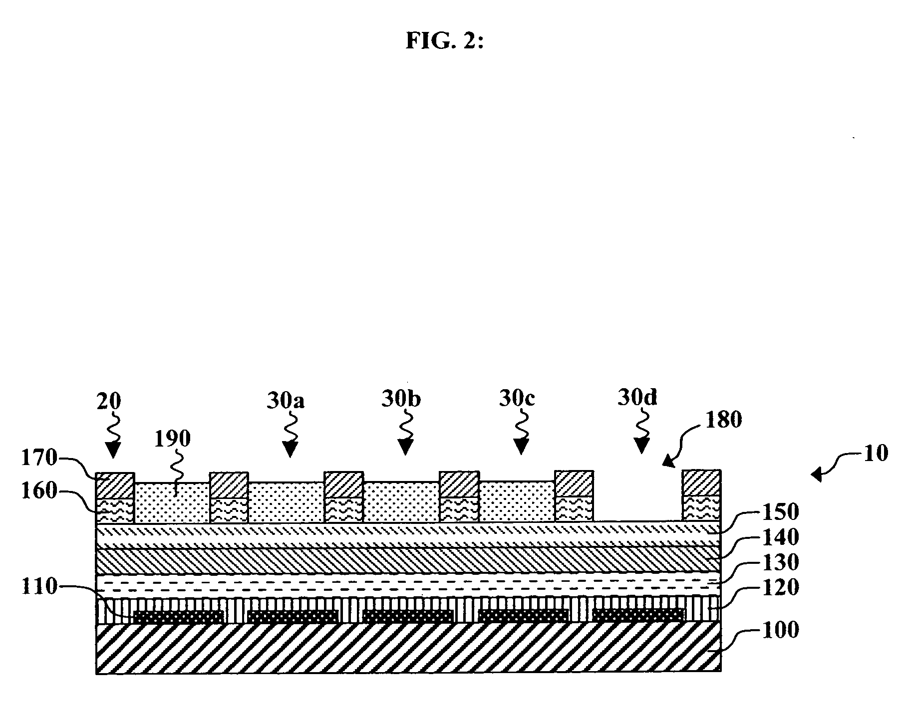
Patterning OLED device electrodes and optical material
a technology of oled devices and electrodes, applied in the field of organic light-emitting diodes (oled) displays, can solve the problems of thermal coefficient of expansion mismatch between shadow masks, difficult handling of large substrates, thin, etc., and achieve improved contrast, improved usability, and improved electrical conductivity
- Summary
- Abstract
- Description
- Claims
- Application Information
AI Technical Summary
Benefits of technology
Problems solved by technology
Method used
Image

Examples
Embodiment Construction
[0027] The term “OLED display” or “organic light-emitting display” is used in its art-recognized meaning of a display device comprising organic light-emitting diodes as pixels. A color OLED display emits light of at least one color. The term “multicolor” is employed to describe a display panel that is capable of emitting light of a different hue in different areas. In particular, it is employed to describe a display panel that is capable of displaying images of different colors. These areas are not necessarily contiguous. The term “full color” is employed to describe multicolor display panels that are capable of emitting in several regions of the visible spectrum and therefore displaying images in a large combination of hues. The red, green, and blue colors constitute the three primary colors from which all other colors can be generated by appropriate mixing. However, for this invention, full-color can include additional different color pixels. The term “hue” refers to the intensity...
PUM
 Abstract
Description
Claims
Application Information