Transistor with workfunction-induced charge layer

a charge layer and transistor technology, applied in the field of field-effect transistors, can solve the problems of limiting the peak doping level and the abruptness of the doping profile, reducing the on-resistance, and increasing the short-channel effect, so as to achieve the effect of enhancing the conductivity between the semiconductor channel and the channel tap

a charge layer and transistor technology, applied in the field of field-effect transistors, can solve the problems of limiting the peak doping level and the abruptness of the doping profile, reducing the on-resistance, and increasing the short-channel effect, so as to achieve the effect of enhancing the conductivity between the semiconductor channel and the channel tap

US6891234B1Active Publication Date: 2005-05-10ACORN SEMI LLC

Image

  • Transistor with workfunction-induced charge layer
  • Transistor with workfunction-induced charge layer
  • Transistor with workfunction-induced charge layer

Examples


Embodiment Construction

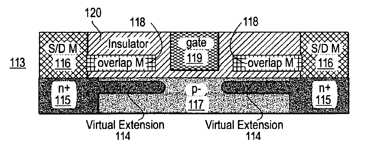
[0045]As is discussed in detail below, the present inventors have developed a FET that includes an extension region which is sufficiently shallow, has a high charge density for low resistance, does not suffer from the decrease in performance (in particular switching speed) as has been reported for other FETs, and does not add significantly to circuit complexity. More specifically, disclosed herein is an electrical switching device (a transistor) that includes one or more conductors (which often will be a metal), each of which overlaps a region of semiconductor between a channel tap (for example, source or drain) region and the channel region. This region of semiconductor, part or all of which is overlapped by the conductor, is a so-called “extension region”. Furthermore, each of these conductor(s) is locally separated from the semiconductor it overlaps by an insulator. Each conductor is electrically isolated from the gate(s) and is chosen to have a workfunction that will induce a de...


PUM


Abstract

An electrical switching device includes a semiconductor having a channel therein which is proximate to at least on channel tap in an extension region and also to a gate. A conductor (e.g., a metal) is disposed proximate to the extension region but is electrically isolated from both the extension region and the gate (e.g., through the use of one or more insulators). The conductor has a workfunction outside of the bandgap of a semiconductor in the extension region and therefore includes a layer of charge in the extension region. The magnitude and polarity of this layer of charge is controlled through selection of the metal, the semiconductor, and the insulator.

Description

RELATED APPLICATIONS[0001]The present application is related to and hereby claims the priority benefit of U.S. Provisional Patent Application 60 / 535,082, entitled “Transistor with Workfunction-Induced Charge Layer”, filed Jan. 7, 2004, incorporated herein by reference.FIELD OF THE INVENTION[0002]The present invention relates generally to solid-state switching and amplification devices and, more particularly, to a field-effect transistor having a layer of charge induced in the conduction path between the channel and one or more channel taps (the source and / or drain in a conventional field-effect transistor) by proximity to a conductor (e.g., a metal) possessing a workfunction outside of the bandgap of the semiconductor in the region in which the charge is induced.BACKGROUND[0003]As the gate length of transistors continues to shrink, the source (and / or drain) region(s) become(s) more of a factor in MOSFET (metal oxide semiconductor field effect transistor) performance. MOSFET scaling ...

Claims


Application Information

Patent Timeline
10 May 2005
Publication
US6891234B1
IPC
H01L21/02; H01L21/336; H01L29/417; H01L29/02; H01L29/08; H01L29/78; H01L29/66; H01L29/49; H01L29/40
CPC
H01L29/0847; H01L29/41725; H01L29/7831; H01L29/66643; H01L29/4983
Inventors
CONNELLY, DANIEL J.; FAULKNER, CARL