Special-shaped tapered double-sided key board manufacturing method

A production method and key board technology, which are used in chemical/electrolytic methods to remove conductive materials, printed circuit manufacturing, electrical components, etc. problem, to achieve the effect of independent connectivity

Active Publication Date: 2016-09-28
KUNSHAN QUANYING ELECTRONICS CO LTD
View PDF3 Cites 1 Cited by
  • Summary
  • Abstract
  • Description
  • Claims
  • Application Information

AI Technical Summary

Problems solved by technology

However, for printed circuit boards with different thicknesses of copper foil, etching on both sides at the same time cannot meet the requirements. At present, the common methods are: one is that the amount of line etching compensation on both sides is based on the thicker copper foil thickness to avoid equal compensation, and then etch The other is to make circuit etching compensation according to the actual copper foil thickness on both sides, and

Method used


Image

  • Special-shaped tapered double-sided key board manufacturing method
  • Special-shaped tapered double-sided key board manufacturing method

Examples


Embodiment Construction

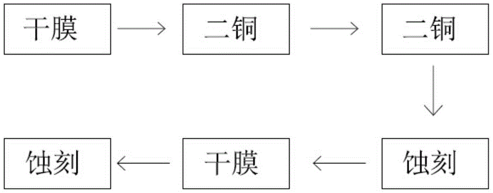
[0020] Such as figure 1 As shown, the manufacturing method of the special-shaped tower-type double-sided key board of the present invention discloses a manufacturing method of a double-sided key board with different copper thickness, which includes the following steps:

[0021] S1 (dry film): First, dry film is applied on the parts that need to be thickened on each bottom copper surface of the key board, so as to produce a stable substance that adheres to the bottom copper surface;

[0022] S2 (second copper): After the dry film, electroplating is performed on various parts of the key board to form a layer of metal film;

[0023] S3 (dry film): Then cover the special-shaped bottom copper surface, and make a pattern on the same-type bottom copper surface;

[0024] S4 (etching): Then confirm that the thickness of the same-sex bottom copper is normally negatively etched;

[0025] S5 (dry film): Then cover the etched bottom copper surface of the same sex, and then make a pattern...


PUM


Abstract

The invention provides a special-shaped tapered double-sided key board manufacturing method. The method comprises the steps that S1 (film drying) film drying is carried out on parts needing thickening on each bottom copper surface of a key board, so as to produce a stable material adhered on each bottom copper surface; S2 (pattern plating) after film drying, each part of the key board is plated to form a metal film; S3 (film drying) then different-shaped bottom copper surfaces are covered and same-shaped bottom copper surfaces are profiled; S4 (etching) normal thickness negative film etching of bottom copper with confirmed same-shaped bottom is carried out; S5 (film drying) etched same-shaped bottom copper surfaces are covered, and different-shaped bottom copper surfaces are patterned; and S6 (etching) normal thickness negative film etching of confirmed different-shaped bottom copper is carried out. According to the invention, front and back copper foils of a printed circuit board are different; tapered layout of the copper foil thickness is realized; high frequency and low frequency coexistence is realized; the method is suitable for double sides of the circuit board; and each side of the circuit board is independent, and can be independently communicated.

Description

technical field [0001] The invention relates to the technical field of circuit boards, in particular to a method for manufacturing a special-shaped tower-type double-sided key board. Background technique [0002] In the production of printed circuit boards, the etching process is an indispensable and important step, especially with the rapid development of microelectronics technology, the wide application of large-scale integrated circuits and ultra-large-scale integrated circuits, making printed circuit boards The width and spacing of the wires are getting smaller and smaller, the wiring density and precision are getting higher and higher, and higher and stricter requirements are put forward for the precision and tolerance of etching. The quality of etching directly affects the quality of printed circuit boards. inferior. [0003] For printed circuit boards with the same thickness of copper foil, usually both sides are etched at the same time to meet the requirements. How...

Claims


Application Information

Patent Timeline
IPC IPC(8): H05K3/06
CPCH05K3/06H05K2203/0369
Inventor 李高猛朱晓菲张海军王恒星孙坤坤刘攀
Owner KUNSHAN QUANYING ELECTRONICS CO LTD
Why Eureka
Try Eureka