Coaxial adjustment device and coaxial adjustment method using the same

An adjustment device, coaxial technology, which is applied in the manufacture of electrical components, circuits, semiconductor/solid-state devices, etc., can solve problems such as coaxial adjustment

Active Publication Date: 2019-12-24
ACM RES SHANGHAI
View PDF5 Cites 0 Cited by
  • Summary
  • Abstract
  • Description
  • Claims
  • Application Information

AI Technical Summary

Problems solved by technology

[0006] In order to solve the above-mentioned technical problems encountered in actual production, the present invention provides a coaxial adjustment device, by adding accessories and carrying out special structural design on the accessories to make them meet certain requirements, combined with laser positioning technology, it can be solved together Solved the problem of coaxial adjustment of wafer fixed plate and shower head in SFP process equipment

Method used


Image

  • Coaxial adjustment device and coaxial adjustment method using the same
  • Coaxial adjustment device and coaxial adjustment method using the same
  • Coaxial adjustment device and coaxial adjustment method using the same

Examples


specific Embodiment approach

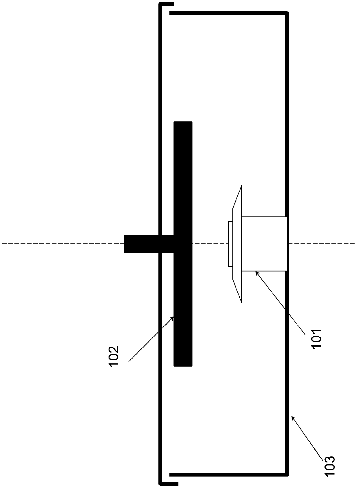
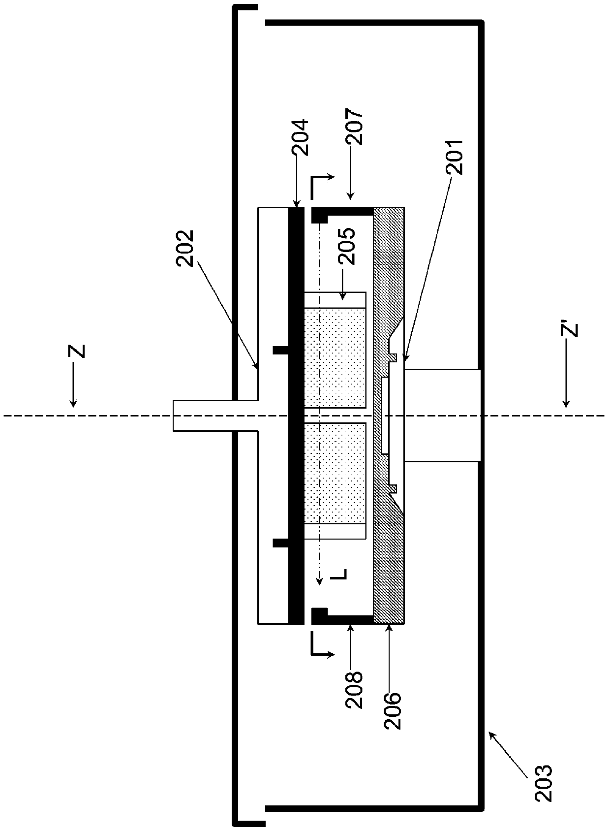
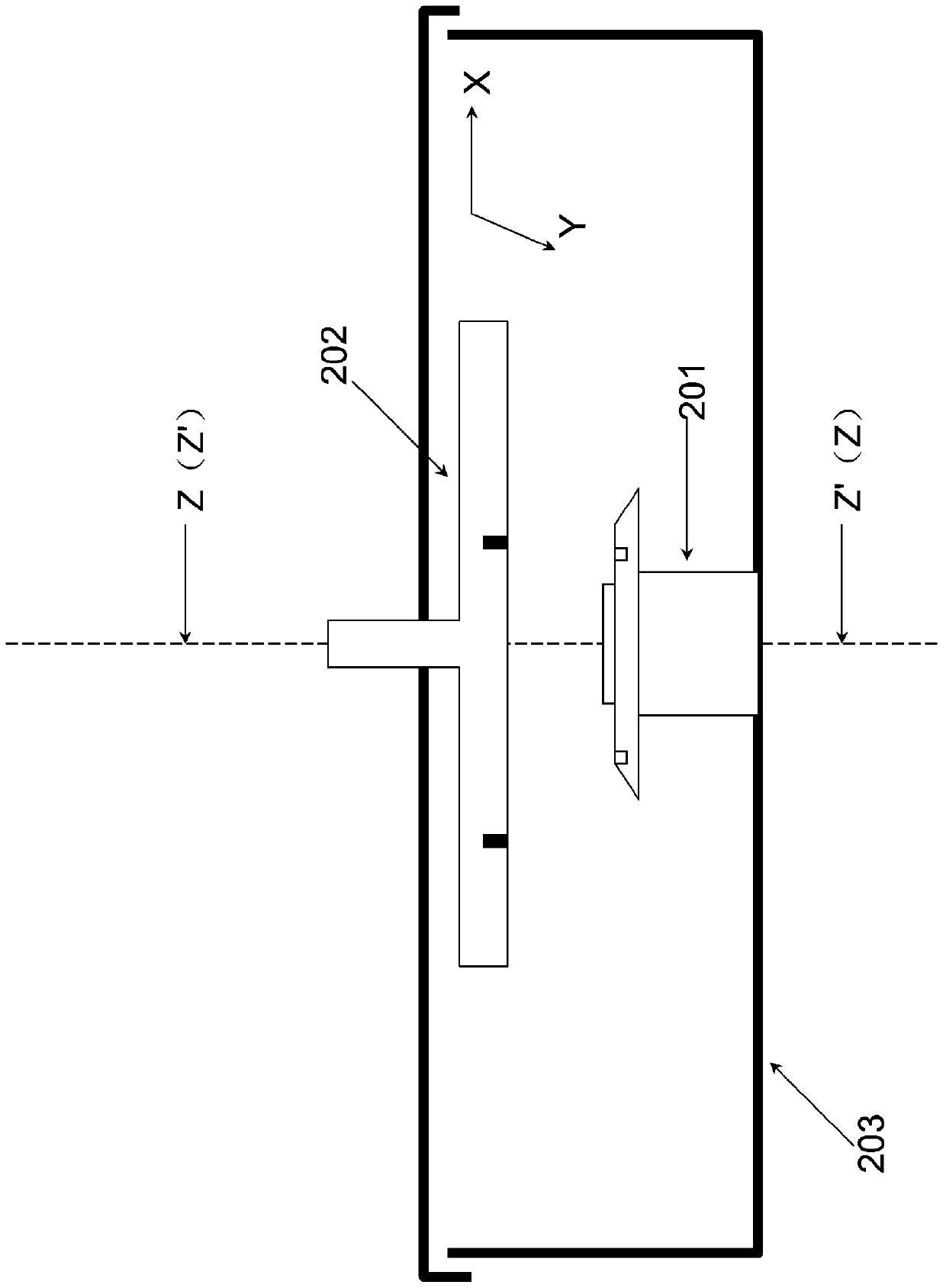
[0061] A method for coaxially adjusting wafer fixation 202 and showerhead 201 using the coaxial adjustment device of Embodiment 1, comprising steps:

[0062] Install the positioning plate 204 on the wafer fixing plate 202 according to the manner determined by the positioning hole 209 and the positioning pile 212;

[0063] Install the positioning seat 206 on the nozzle 201 according to the manner determined by the first set of mounting holes 210 and the positioning column 215;

[0064] Turn on the laser device, and emit the laser beam directionally from the transmitting part 207 of the laser device to the receiving part 208;

[0065] Adjust the horizontal position and the vertical position of the wafer fixing plate 202 so that the laser beam falls into the shielding area of ​​the shield 205 and directly strikes the shield 205 along a direction parallel to the X axis; the wafer fixing plate 202 is controlled to drive the positioning plate 204 Translate along the Y-axis until th...


PUM


Abstract

The invention, which relates to the semiconductor production and processing field, provides a coaxial adjusting device for carrying out coaxial adjustment on a wafer fixing plate and a nozzle in a semiconductor device. The coaxial adjusting device is composed of a wafer fixing plate, a positioning plate, a positioning seat, a nozzle, and a laser device. The wafer fixing plate can rise or decline in a vertical direction and can move horizontally in a horizontal direction along an X axis and a Y axis. Positioning holes are formed in the wafer fixing plate and are used for installing the positioning plate. A shielding object is arranged below the positioning plate; at least two slits are formed in the shielding object; and the intersection line of the two slits is located at a central axis Z of the wafer fixing plate. Mounting holes are formed in the nozzle; the positioning seat is installed at the nozzle by the mounting holed and positioning posts; and an emission part and a receiving part of the laser device are carried by the positioning seat.

Description

technical field [0001] The invention belongs to the field of semiconductor processing and manufacturing, and more specifically relates to a device and method for precisely positioning a wafer fixed plate and a spray head during wafer processing. Background technique [0002] The semiconductor industry has entered an upward channel of rapid development. The high-precision semiconductor technology based on the TSV process is highly praised by the majority of chip manufacturers. Correspondingly, the corresponding semiconductor processing technology has also begun another round of innovation. [0003] In order to obtain higher quality wafer products, it is necessary to perform stress-free chemical polishing (SFP process) on some wafers, and it is necessary to grind the wafer surface to achieve the corresponding thickness. figure 1 The processing equipment used in the SFP process is given. The equipment includes a process chamber 103 , a showerhead 101 protrudes below the proces...

Claims


Application Information

Patent Timeline
Patent Type & Authority Patents(China)
IPC IPC(8): H01L21/68H01L21/67H01L21/02
Inventor 代迎伟金一诺王坚王晖
Owner ACM RES SHANGHAI
Why Eureka
Try Eureka