Component mounting line, component mounting method and component mounting apparatus

A technology of installation device and installation method, applied in the direction of electrical components, electrical components, circuit inspection/monitoring/correction, etc., which can solve the problems of undisclosed, specified and mounted appropriateness

Active Publication Date: 2016-10-12
PANASONIC INTELLECTUAL PROPERTY MANAGEMENT CO LTD
View PDF5 Cites 4 Cited by
  • Summary
  • Abstract
  • Description
  • Claims
  • Application Information

AI Technical Summary

Problems solved by technology

[0006] However, the prior art including Patent Document 1 does not disclose a specific method for specifying an appropriate size of the mounted solder sheet when mounting the solder sheet on the board in the component mounting device.
Therefore, there is a problem that it is difficult to specify and mount solder flakes of an appropriate size for each of the several hundred to several thousand pads on the substrate.

Method used


Image

  • Component mounting line, component mounting method and component mounting apparatus
  • Component mounting line, component mounting method and component mounting apparatus
  • Component mounting line, component mounting method and component mounting apparatus

Examples


Embodiment Construction

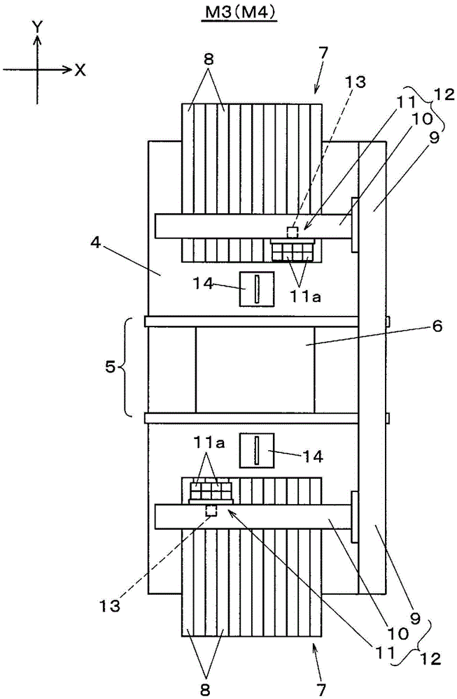
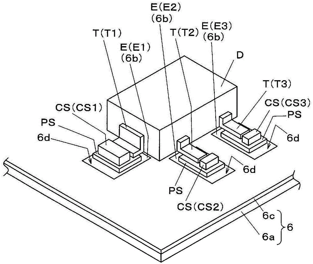
[0047] Next, embodiments of the present invention will be described with reference to the drawings. Below, the substrate transport direction ( figure 2 The left and right direction of the paper) is defined as the X direction, and the direction perpendicular to the X direction in the horizontal plane ( figure 2 The up and down direction of the paper) is defined as the Y direction.

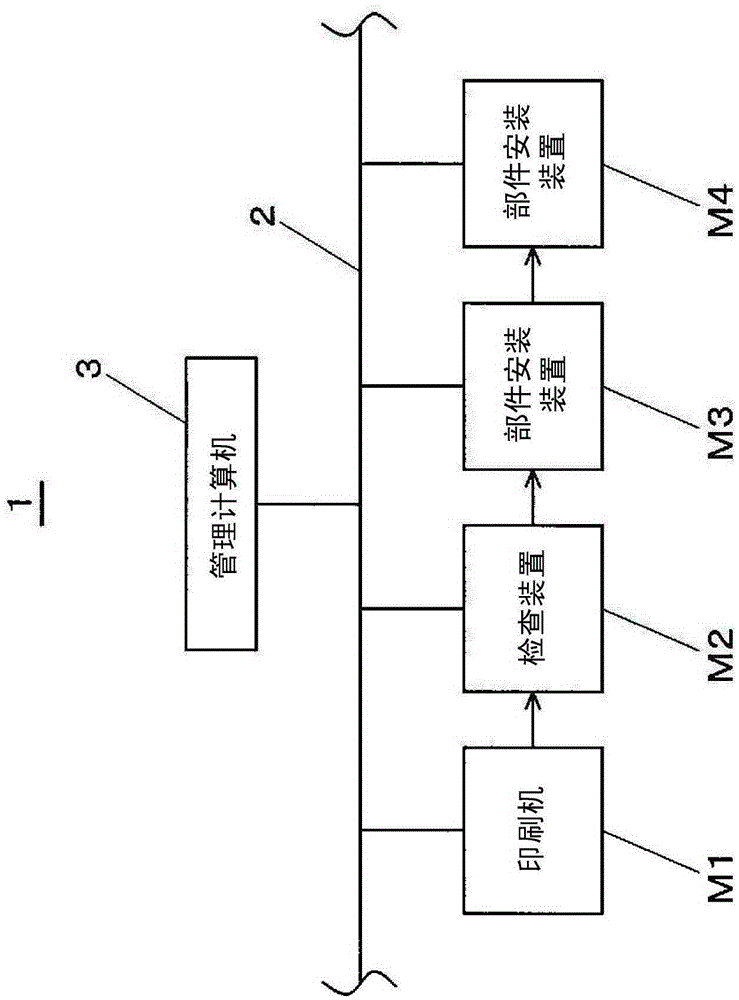
[0048] First, refer to figure 1 The component mounting line 1 will be described. exist figure 1 Among them, the component mounting production line 1 is configured by connecting a plurality of components mounting devices, that is, a printing machine M1, an inspection device M2, and a component mounting device M3, M4, and connecting the devices through a communication network 2 and controlling them by a management computer 3. overall.

[0049] The printer M1 has a function of transferring paste-like cream solder on pads formed on a substrate via a metal mask by screen printing. The inspection ...


PUM


Abstract

A component mounting line, a component mounting method, and a componetn mounting apparauts are provided for supporting a sheet soldering flux in proper size onto a substrate. The component mounting line includes an inspecting apparatus and a component mounting apparatus. The inspecting apparatus measures a solder volume of a printed solder on each electrode of a board. The component mounting apparatus includes a mounting unit that mounts an electronic component on the board, at least one component supply unit that supplies a chip solder, and a control unit that controls the mounting unit to mount the chip solder supplied from the component supply unit based on production data in which a size of the chip solder is instructed corresponding to the solder volume measured for each of component terminals corresponding to each electrode of the board.

Description

technical field [0001] The present invention relates to a component mounting production line for mounting components on a substrate, a component mounting method, and a component mounting device. Background technique [0002] In the manufacture of mounting substrates in which electronic components (hereinafter referred to as "components") are mounted on substrates, the electrodes (hereinafter referred to as "lands") for component bonding on the substrate are connected via a metal mask using a printing machine. ".) Transfer cream solder, mount components on the substrate with a component mounting device, and then melt the cream solder by reflow soldering to join component terminals to pads. In recent years, with the miniaturization of components and narrower pitch of component terminals, the opening area of ​​metal masks has become smaller, and the metal masks have been thinned in order to cope with printing defects caused by deterioration of solder shortage. [0003] However...

Claims


Application Information

Patent Timeline
Patent Type & Authority Applications(China)
IPC IPC(8): H05K13/04
CPCH05K13/04H05K3/1216H05K2203/16H05K13/0817H05K13/0465H05K13/08
Inventor 伊藤克彦池田政典冈本健二
Owner PANASONIC INTELLECTUAL PROPERTY MANAGEMENT CO LTD
Why Eureka
Try Eureka