Display panel, display panel test system and test method of display panel

A display panel and test method technology, applied to static indicators, instruments, etc., can solve the problems that it is difficult to obtain the real impedance of thin film transistors, and the volt-ampere characteristic curve cannot be truly reflected, and achieve the effect of consistent impedance characteristics

Active Publication Date: 2016-11-09
TCL CHINA STAR OPTOELECTRONICS TECH CO LTD
View PDF5 Cites 6 Cited by
  • Summary
  • Abstract
  • Description
  • Claims
  • Application Information

AI Technical Summary

Problems solved by technology

Because the design of the test point is only a simulation test, it is difficult to obtain the real impedance of the thin film transistor, which makes it impossible to truly reflect the volt-ampere characteristic curve of the pixel structure in the effective display area of ​​the display panel, and there is an RC delay in the real in-plane volt-ampere characteristic curve test
Existing RC delay effects are only simulated by design software

Method used


Image

  • Display panel, display panel test system and test method of display panel
  • Display panel, display panel test system and test method of display panel
  • Display panel, display panel test system and test method of display panel

Examples


Embodiment Construction

[0023] The present invention will be described in detail below in conjunction with the accompanying drawings and embodiments.

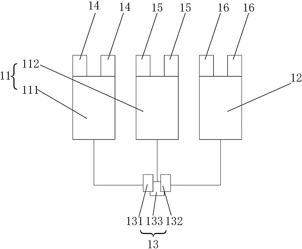
[0024] see figure 1 , figure 1 It is a schematic diagram of the structural principle of a preferred embodiment of the display panel of the present invention. In this embodiment, the display panel includes: an in-plane TFT 11 , a pixel electrode layer 12 , a TFT for testing 13 , a first metal layer test terminal 14 , a second metal layer test terminal 15 and a pixel electrode layer test terminal 16 .

[0025] Both the in-plane thin film transistor 11 and the pixel electrode layer 12 are located inside the display panel, and the in-plane thin film transistor 11 includes a first metal layer 111 and a second metal layer 112 . The display panel includes two opposing substrates, such as a thin film transistor array substrate and a color filter substrate. The in-plane thin film transistor 11 and the pixel electrode layer 12 are both located on the thin fil...


PUM


Abstract

The invention discloses a display panel, a display panel test system and a test method of a display panel. The display panel comprises an in-plane thin film transistor, a pixel electrode layer, first metal layer test terminals, second metal layer test terminals and pixel electrode layer test terminals, wherein the in-plane thin film transistor comprises a first metal layer and a second metal layer, a first pathway end of a test thin film transistor is electrically connected with a first end portion of the first metal layer, a second pathway end is connected electrically with a first end portion of the pixel electrode layer, a control end is electrically connected with a first portion of the second metal layer, the first metal layer test terminals are electrically connected with a second end portion of the first metal layer, the second metal layer test terminals are electrically connected with a second end portion of the second metal layer, the pixel electrode layer test terminals are connected electrically with a second end portion of the pixel electrode layer, and the first metal layer test terminals, the second metal layer test terminals and the pixel electrode layer test terminals are used for connection with test equipment. According to the invention, real impedance of the in-plane thin film transistor of the display panel can be tested and estimated.

Description

technical field [0001] The present invention relates to the technical field of display panel testing, in particular to a display panel, a display panel testing system and a display panel testing method. Background technique [0002] TEG electrical test is a test to be carried out before the display panel leaves the factory. In order to perform TEG electrical test, the circuit layout design of the existing display panel products is the test point designed outside the test surface when testing the volt-ampere characteristic curve of the pixel structure. , judge whether the volt-ampere characteristic curve meets the process requirements through the test results of the test points. Because the test point design is only a simulation test, it is difficult to obtain the real impedance of the thin film transistor, which makes it impossible to truly reflect the volt-ampere characteristic curve of the pixel structure in the effective display area of ​​the display panel, and there is R...

Claims


Application Information

Patent Timeline
Patent Type & Authority Applications(China)
IPC IPC(8): G09G3/00
CPCG09G3/006
Inventor 陈建超
Owner TCL CHINA STAR OPTOELECTRONICS TECH CO LTD
Why Eureka
Try Eureka