
tem sample preparation method

A sample and semiconductor technology, which is applied in the field of TEM sample preparation, can solve the problems that it is difficult to obtain a clear high-resolution TEM image, the sample is easy to bend, and the image is blurred, etc., so as to achieve the effect of clear TEM image

Active Publication Date: 2019-04-02
SEMICON MFG INT (SHANGHAI) CORP
View PDF9 Cites 0 Cited by
  • Summary
  • Abstract
  • Description
  • Claims
  • Application Information

AI Technical Summary

Problems solved by technology

[0004] However, in the prior art, the TEM sample prepared by FIB is easy to bend due to the thinness of the sample (thickness is usually less than 100nm), and it is difficult for the electron beam to hit the sample vertically during the TEM test, thus making the test The image is blurred, and it is more difficult to obtain a clear high-resolution TEM image

Method used


Image

  • tem sample preparation method
  • tem sample preparation method
  • tem sample preparation method

Examples


Embodiment Construction

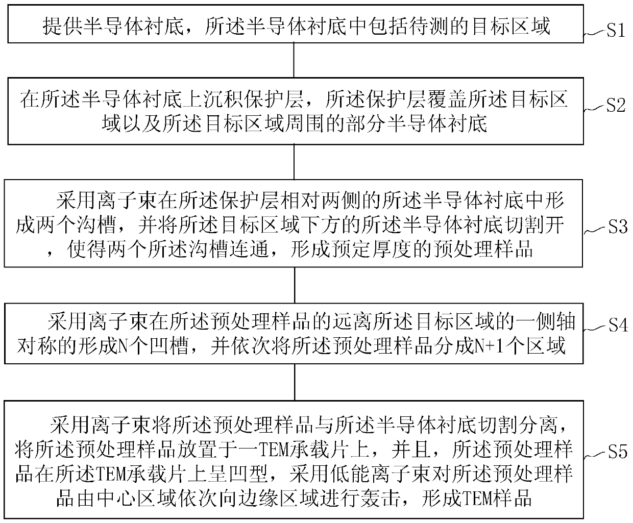
[0033] As mentioned in the background art, the pretreated sample after FIB cutting and thinning is prone to bending phenomenon, resulting in blurred test images. For this reason, the present invention provides a kind of preparation method of TEM sample, uses ion beam to form a plurality of grooves in the pretreatment sample, and the groove releases the stress of the pretreatment sample, after that, the pretreatment sample is placed on the TEM bearing in a concave shape. On the chip, a low-energy ion beam is used to bombard the pretreated sample symmetrically from the center area to the edge area in sequence. Due to the impact of the ion beam, the pretreated sample is sequentially attached to the TEM carrier sheet, and finally it is completely attached to the TEM carrier sheet. combine. In this way, when observed by TEM, the transmitted electrons can be perpendicular to the TEM sample, so that the imaging is clear, thereby improving the quality of TEM imaging.

[0034] figure...


PUM

PropertyMeasurementUnit
depthaaaaaaaaaa
widthaaaaaaaaaa
thicknessaaaaaaaaaa

Abstract

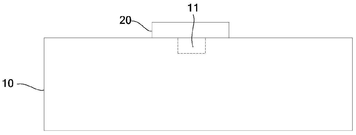
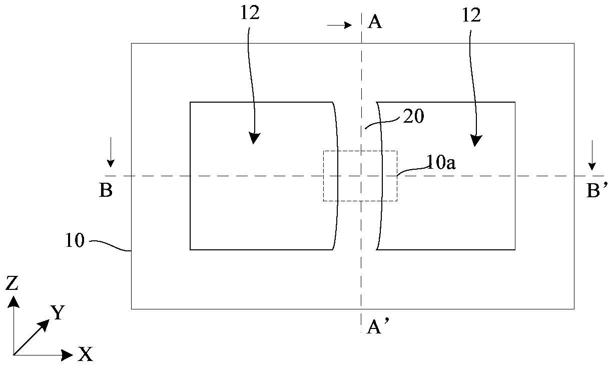
The invention provides a production method of a TEM sample. The method comprises the following steps: providing a semiconductor substrate comprising a target area to be detected; depositing a protection layer covering the target area; respectively forming trenches in semiconductor substrates at two opposite sides of the protection layer, and cutting the semiconductors under the target area to make the two trenches be connected in order to form a preprocessed sample; forming N grooves in the preprocessed sample to sequentially divide the preprocessed sample into N+1 areas; and cutting to separate the preprocessed sample from the semiconductor substrate, placing the preprocessed sample on a TEM carrier sheet in a concave form, and sequentially bombarding the preprocessed sample from the center area to the edge areas by adopting low-energy ion beams in order to form the TEM sample. The formed TEM sample is completely applied to the TEM carrier sheet, so the electron beams are vertically incident to the TEM sample.

Description

technical field [0001] The invention relates to the technical field of surface detection and analysis, in particular to a method for preparing a TEM sample. Background technique [0002] With the development of semiconductor technology, the size of semiconductor devices is gradually reduced in proportion, and their critical dimensions become smaller and smaller, gradually from 90nm to 45nm to 28nm. For semiconductor devices with smaller and smaller critical dimensions, focused plasma beam (FIB) and nanomanipulator (Omniprobe) are usually used to prepare transmission electron microscope (TEM) samples, because Omniprobe is used with FIB to prepare samples, samples It can be made very thin, so that the electron beam can pass through the sample, and meet the requirements of morphology analysis for TEM observation of critical dimensions. [0003] The FIB sample preparation process includes a series of FIB grinding and sample moving steps, specifically, the TEM sample is first se...

Claims


Application Information

Patent Timeline
Patent Type & Authority Patents(China)
IPC IPC(8): G01N1/28
Inventor 殷原梓
Owner SEMICON MFG INT (SHANGHAI) CORP
Learn More