Cover plate, preparation method of cover plate and display device
A cover plate and display panel technology, which is applied in optics, instruments, electrical digital data processing, etc., can solve the problems of multiple patterning processes, increased production costs, and affecting product performance, so as to improve performance, increase transmittance, The effect of high yield
- Summary
- Abstract
- Description
- Claims
- Application Information
AI Technical Summary
Problems solved by technology
Method used
Image
Examples
preparation example Construction
[0065] The embodiment of the present invention also provides a method for preparing a cover plate, as shown in FIG. 8(a), including the following steps:
[0066] S10 , forming a first electrode layer on the transparent substrate 41 through a patterning process; the first electrode layer includes a plurality of first electrodes, and the first electrodes have a grid structure.
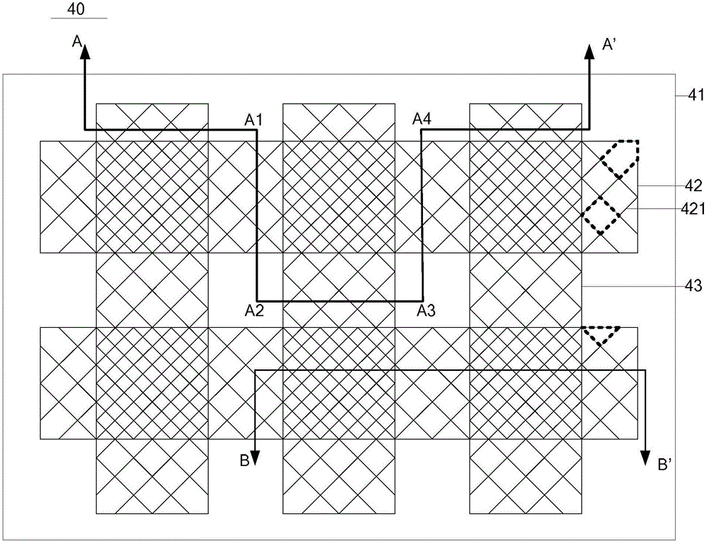
[0067] Among them, refer to Figure 2-Figure 4 As shown, the first electrode may be, for example, the sensing electrode 42 , and in this case the first electrode layer is the sensing electrode layer.
[0068] Here, the patterning process is not limited to patterning using a mask, and may also include other patterning methods such as printing and printing. That is, in the embodiments of the present invention, any process that can form the first electrode layer can be called a patterning process.
[0069] S11. Reference Figure 3-Figure 4 As shown, an insulating layer 44 is formed on the transparent sub...
Embodiment 1
[0078] Embodiment 1: a preparation method of a cover plate, as shown in Figure 8(b), comprises the following steps:
[0079] S101 , forming a first conductive film on the transparent substrate 41 .
[0080] Wherein, the first conductive thin film may be formed by various methods such as deposition, coating, sputtering and the like.
[0081] S102, forming a photoresist on the first conductive film.
[0082] Wherein, the photoresist can be formed by deposition, coating and the like.
[0083] S103 , placing a mask on the photoresist, exposing and developing the photoresist, so that the remaining photoresist corresponds to the first electrode to be formed into the first electrode layer.
[0084] Among them, refer to Figure 2-Figure 4 As shown, the first electrode may be, for example, the sensing electrode 42 , and in this case the first electrode layer is the sensing electrode layer.
[0085] S104. Etching the first conductive film not covered by the photoresist to form the f...
Embodiment 2
[0097] Embodiment 2, a preparation method of a cover plate, as shown in FIG. 8(c), includes the following steps:
[0098]S201 , forming a first electrode layer on the transparent substrate 41 through a printing process or a printing process; the first electrode layer includes a plurality of first electrodes, and the first electrodes are in a grid structure.
[0099] Among them, refer to Figure 2-Figure 4 As shown, the first electrode may be, for example, the sensing electrode 42 , and in this case the first electrode layer is the sensing electrode layer.
[0100] S202. Reference Figure 3-Figure 4 As shown, an insulating film is coated on the transparent substrate formed with the first electrode layer to form the insulating layer 44 .
[0101] S203, forming a second electrode layer on the insulating layer 44 through a printing process or a printing process; the second electrode layer includes a plurality of second electrodes, the second electrodes are in a grid structure, t...
PUM
 Abstract
Description
Claims
Application Information


