Supercharge Your Innovation With Domain-Expert AI Agents!

Mainboard, mobile terminal and mainboard manufacturing method

A manufacturing method and motherboard technology, applied in printed circuit manufacturing, electrical components, printed circuits, etc., can solve problems such as damage to electronic component pins

Inactive Publication Date: 2017-02-15
SHANGHAI GREEN ORANGE IND
View PDF3 Cites 0 Cited by
  • Summary
  • Abstract
  • Description
  • Claims
  • Application Information

AI Technical Summary

Problems solved by technology

[0005] At present, there is no fixed method to align all the pins of the electronic components with the jacks on the PCB board, which often leads to pressing the electronic components when the pins of the electronic components are not aligned with the jacks on the PCB board, so that the pins of the electronic components cannot be inserted. Connected to the socket of the PCB board, damaging the pins of electronic components

Method used


Image

  • Mainboard, mobile terminal and mainboard manufacturing method
  • Mainboard, mobile terminal and mainboard manufacturing method
  • Mainboard, mobile terminal and mainboard manufacturing method

Examples


Embodiment 1

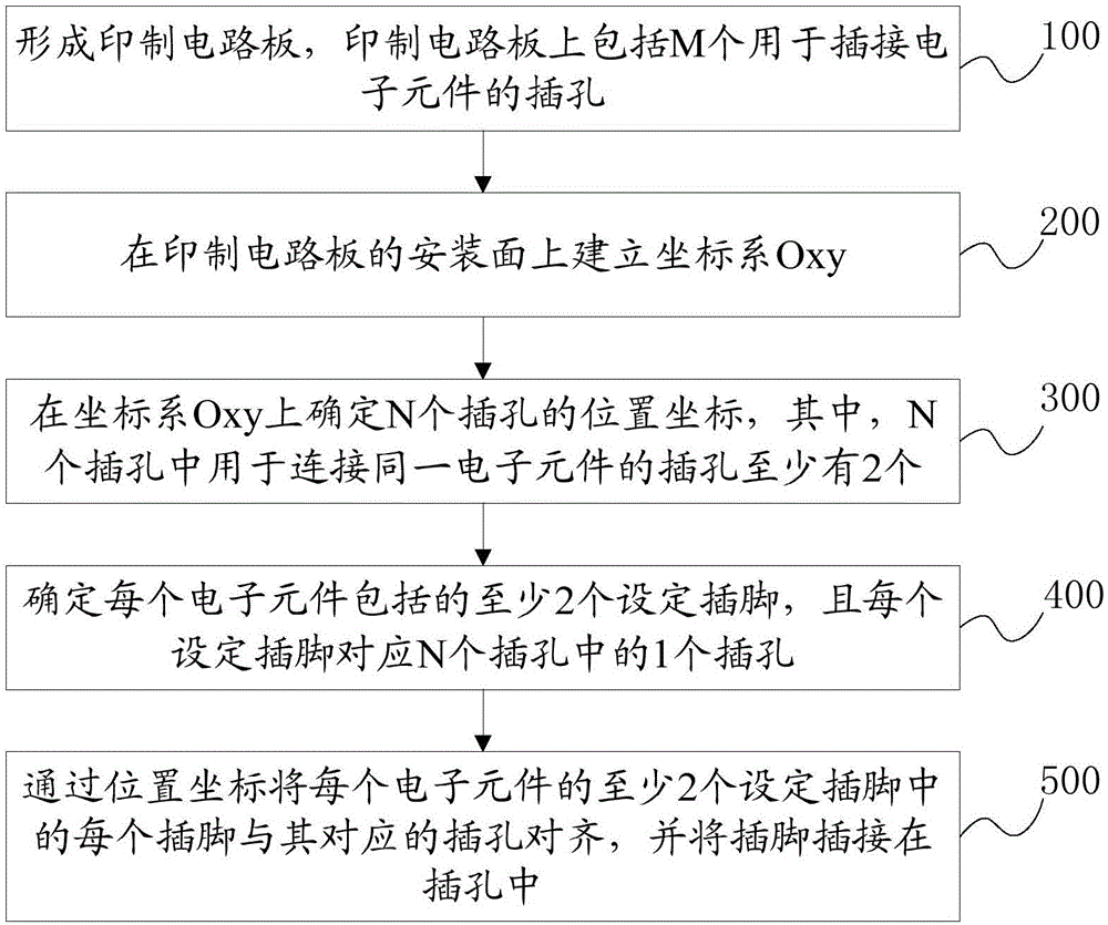
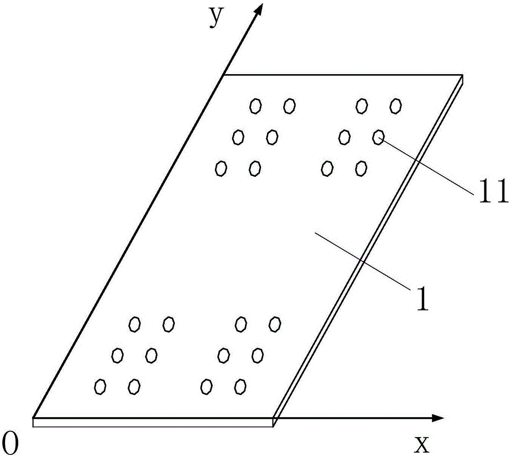
[0034] An embodiment of the present invention provides a method for manufacturing a mainboard, and the execution subject of the method may be an equipment processing center. The following will combine specific implementation methods, figure 1 The processing flow shown is described in detail, and the content can be as follows:

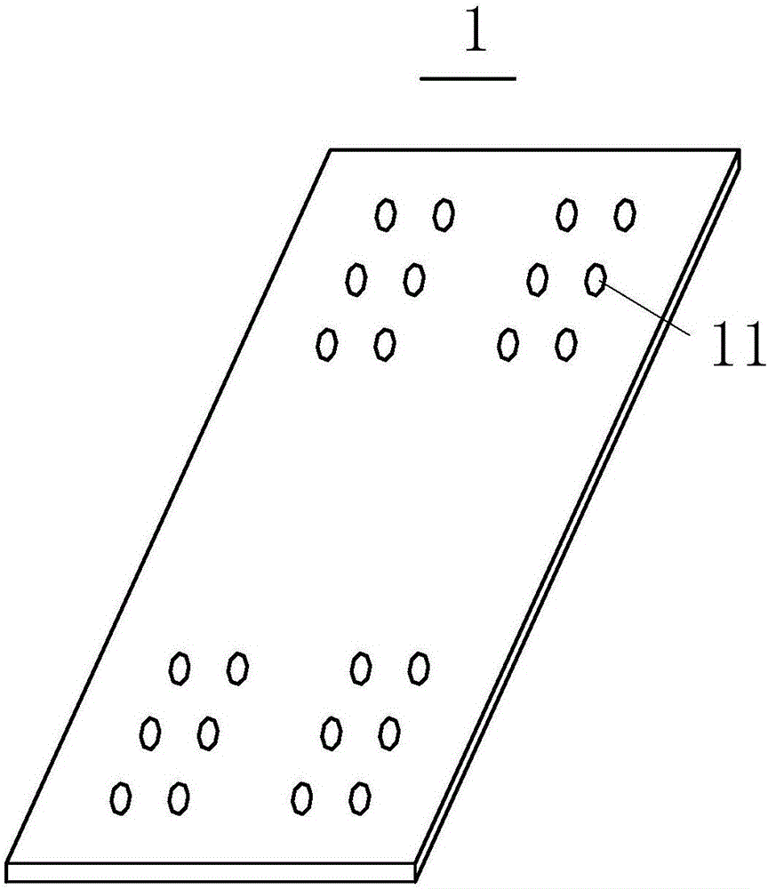
[0035] Step 100, forming a printed circuit board 1, see figure 2 , the printed circuit board 1 includes M jacks 11 for inserting electronic components 2; wherein, M is an integer, and M>2.

[0036] Wherein, the process of forming the printed circuit board 1 is specifically:

[0037] form the substrate;

[0038] forming an insulating layer on the substrate;

[0039] An installation surface is formed on the insulating layer, wherein the installation surface includes a circuit and a plurality of drawing surfaces, and the plurality of drawing surfaces are electrically connected by circuits;

[0040] M sockets 11 for inserting electronic components 2 a...

Embodiment 2

[0057] An embodiment of the present invention provides a main board, and the main board is manufactured according to the manufacturing method for the main board described in the first embodiment.

[0058] The main board provided by the embodiment of the present invention is manufactured by the main board production method described in the first embodiment, so that the production yield of the main board is high, the production cost of the main board is reduced, and the quality of the main board is improved.

Embodiment 3

[0060] An embodiment of the present invention provides a mobile terminal, and the mobile terminal includes the motherboard described in the second embodiment.

[0061] Optionally, the mobile terminal may be a tablet computer or a mobile phone.

[0062] The mobile terminal provided in the embodiment of the present invention adopts the motherboard provided in the second embodiment, so that the production yield of the mobile terminal is high, and the quality of the mobile terminal is improved.


PUM


Abstract

The invention discloses a mainboard, a mobile terminal and a mainboard manufacturing method, and belongs to the technical field of mobile equipment. The method comprises the following steps of: forming a PCB, wherein the PCB includes M jacks used for being inserted by electronic components; establishing a coordinate system Oxy on the installation surface of the PCB; determining position coordinates of N jacks on the coordinate system Oxy, wherein at least two jacks in the N jacks are used for being connected to the same electronic component; determining at least two set insertion pins included by each electronic component, wherein each set insertion pin corresponds to one jack in the N jacks; and, aligning each set insertion pin in the at least two set insertion pins of each electronic component to the corresponding jack, inserting the set insertion pins in the jacks, and thereby, completing installation of the electronic component on the PCB. Alignment of all the electronic components and the jacks on the PCB can be absolutely ensured through the coordinate system Oxy; and thus, the insertion pins of the electronic components can be accurately inserted in the jacks of the PCB.

Description

technical field [0001] The invention relates to the technical field of mobile devices, in particular to a motherboard, a mobile terminal and a method for manufacturing the motherboard. Background technique [0002] With the progress of the times, mobile devices are indispensable communication tools in people's daily work; such as mobile phones and tablet computers, etc., the core electronic components of these mobile devices are installed on the motherboard. [0003] At present, the manufacturing method of the motherboard includes forming a PCB (Printed circuit board, printed circuit) board, aligning all the pins of the electronic components in the jacks on the PCB one by one, pressing the electronic components to insert all the pins of the electronic components on the PCB. On the board, the core electronic components of the mobile device are installed on the motherboard by this method. [0004] In the process of implementing the embodiments of the present invention, the in...

Claims


Application Information

Patent Timeline
Patent Type & Authority Applications(China)
IPC IPC(8): H05K3/30
CPCH05K3/306H05K2203/166
Inventor 蔡正龙刘国政吴旭李辉
Owner SHANGHAI GREEN ORANGE IND
Features
  • R&D
  • Intellectual Property
  • Life Sciences
  • Materials
  • Tech Scout
  • Unparalleled Data Quality
  • Higher Quality Content
  • 60% Fewer Hallucinations
Learn More