Image capturing lens group, image capturing device and electronic device
An image capture and lens group technology, applied in optical components, instruments, optics, etc., can solve the problems of difficult imaging quality and unsatisfactory lens structure, and achieve the effect of expanding the aperture, increasing the amount of light entering, and increasing the symmetry
- Summary
- Abstract
- Description
- Claims
- Application Information
AI Technical Summary
Problems solved by technology
Method used
Image
Examples
no. 1 example
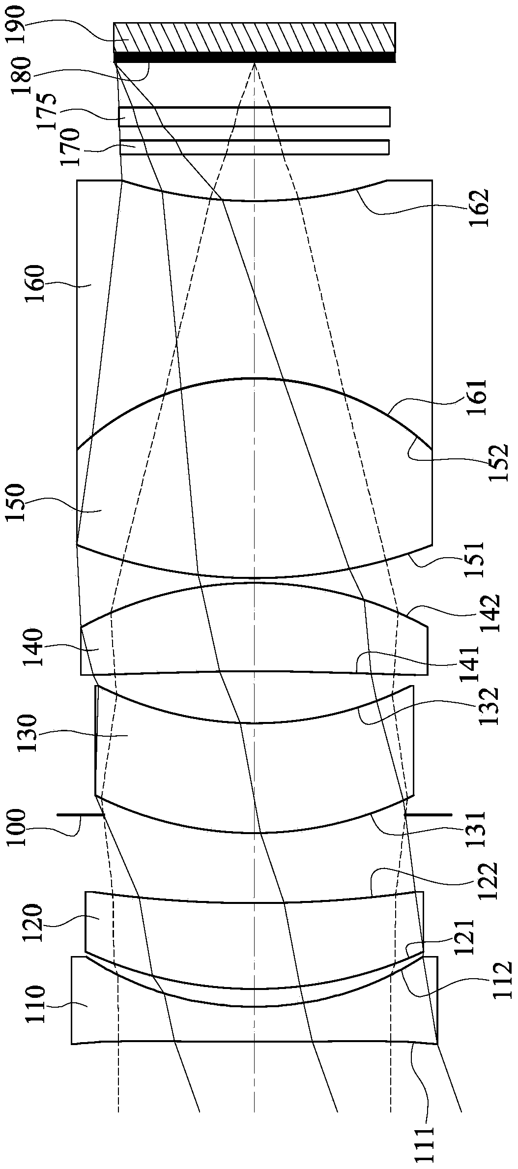
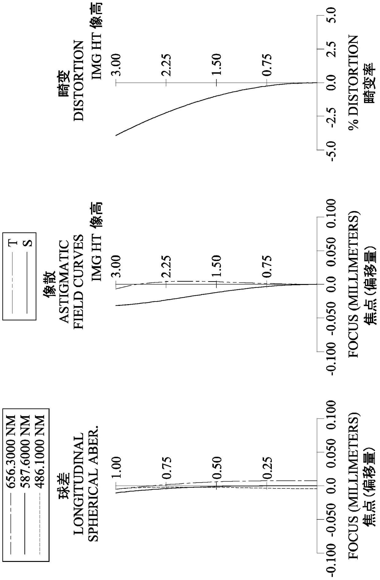
[0145] Please refer to figure 1 and figure 2 ,in figure 1 It is a schematic diagram of an imaging device according to the first embodiment of the present invention, figure 2 From left to right are the spherical aberration, astigmatism and distortion curves of the first embodiment. Depend on figure 1 It can be seen that the image capturing device includes an image capturing lens group (not another number) and an electronic photosensitive element 190 . The image capture lens group includes first lens 110, second lens 120, aperture 100, third lens 130, fourth lens 140, fifth lens 150, sixth lens 160, infrared filter Filter element (IR-cut Filter) 170 , protective glass 175 and imaging surface 180 . Wherein, the electronic photosensitive element 190 is disposed on the imaging surface 180 . There are four single non-bonded lenses (110-140) in the image capture lens group, and two cemented lenses (150-160) in the image capture lens group.
[0146] The first lens 110 has neg...
no. 2 example
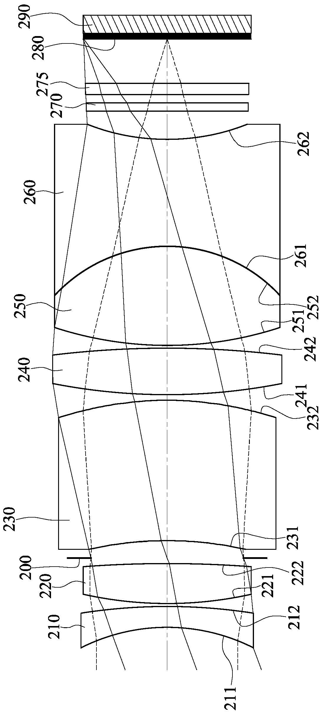
[0189] Please refer to image 3 and Figure 4 ,in image 3 It is a schematic diagram of an imaging device according to a second embodiment of the present invention, Figure 4 From left to right are the spherical aberration, astigmatism and distortion curves of the second embodiment. Depend on image 3 It can be seen that the image capturing device includes an image capturing lens group (not another number) and an electronic photosensitive element 290 . The image capture lens group includes first lens 210, second lens 220, aperture 200, third lens 230, fourth lens 240, fifth lens 250, sixth lens 260, infrared filter The filter element 270 , the protective glass 275 and the imaging surface 280 . Wherein, the electronic photosensitive element 290 is disposed on the imaging surface 280 . There are four single non-bonded lenses (210-240) in the image capture lens group, and two cemented lenses (250-260) in the image capture lens group.
[0190] The first lens 210 has negativ...
no. 3 example
[0203] Please refer to Figure 5 and Image 6 ,in Figure 5 It is a schematic diagram of an imaging device according to a third embodiment of the present invention, Image 6 From left to right are the spherical aberration, astigmatism and distortion curves of the third embodiment. Depend on Figure 5 It can be seen that the image capturing device includes an image capturing lens group (not another number) and an electronic photosensitive element 390 . The image capture lens group includes first lens 310, second lens 320, aperture 300, third lens 330, fourth lens 340, fifth lens 350, sixth lens 360, infrared filter The filter element 370 , the protective glass 375 and the imaging surface 380 . Wherein, the electronic photosensitive element 390 is disposed on the imaging surface 380 . There are four single non-bonded lenses (310-340) in the image capture lens group, and two cemented lenses (350-360) in the image capture lens group.
[0204] The first lens 310 has negative...
PUM
 Abstract
Description
Claims
Application Information


